Method utilizing TSV (Through-Silicon-Via) to realize wafer level package of GaAs (gallium arsenide) image sensor

An image sensor and wafer-level packaging technology, applied in radiation control devices, semiconductor/solid-state device manufacturing, electrical components, etc., can solve the problems of small signal delay, low capacitance value, high cost, etc., and achieve low cost, high interaction Continuous density, no radiation damage effect

Inactive Publication Date: 2012-07-04
SHANGHAI INST OF MICROSYSTEM & INFORMATION TECH CHINESE ACAD OF SCI
View PDF5 Cites 20 Cited by
  • Summary
  • Abstract
  • Description
  • Claims
  • Application Information

AI Technical Summary

Problems solved by technology

[0011] The object of the present invention is to provide a through-silicon via structure for the packaging of an image sensor with higher reliability; to overcome the problem of poor reliability of the above-mentioned T-type connection
[0012] The purpose of the present invention is to provide a wafer-level packaging method for GaAs image sensors using TSV technology, to overcome the high cost of the conventional TSV method, the low capacitance value formed between TSVs, and small signal delay, and there is no radiation to the device at the same time. photo damage; at the same time overcome the problem of poor reliability of the existing T-connection

Method used


Image

  • Method utilizing TSV (Through-Silicon-Via) to realize wafer level package of GaAs (gallium arsenide) image sensor
  • Method utilizing TSV (Through-Silicon-Via) to realize wafer level package of GaAs (gallium arsenide) image sensor
  • Method utilizing TSV (Through-Silicon-Via) to realize wafer level package of GaAs (gallium arsenide) image sensor

Examples


Embodiment Construction

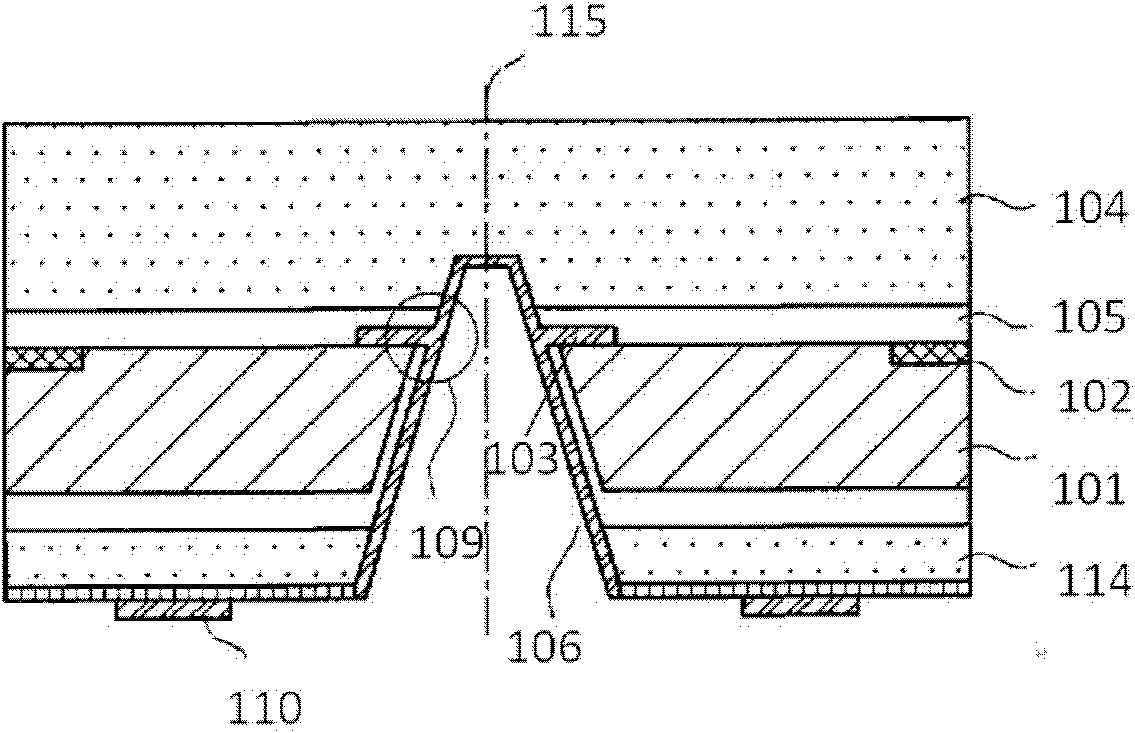
[0041] In order to fully demonstrate the advantages and positive effects of the present invention, the substantive features and remarkable progress of the present invention will be further described below in conjunction with the accompanying drawings and embodiments.

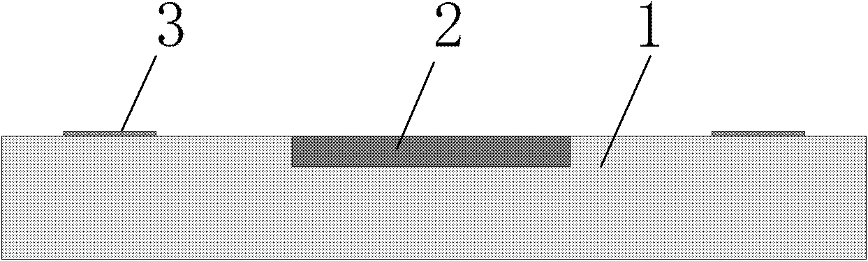
[0042] refer to figure 2 The GaAs image sensor wafer 1 includes several chips, and image sensing components are formed on the front of each chip through a preset manufacturing process, including the formation of image sensing units 2 and pad electrodes 3 . The pad electrode 3 is distributed in the non-functional area around the image sensing unit, and the material selected can be aluminum, gold or copper. The image sensor is used in the visible light range, and the wafer thickness is 350 μm.

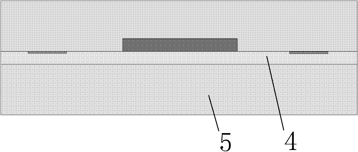
[0043] Thereafter, refer to image 3, bonding the wafer 1 to a transparent substrate 5 . The substrate plays the role of light transmission, protection from external pollution and mechanical damage, and at the same tim...


PUM


Abstract

The invention relates to a method utilizing TSV (Through-Silicon-Via) to realize wafer level package of a GaAs (gallium arsenide) image sensor. The method comprises the following steps: combining wet etching with mechanical machining to machine a groove; manufacturing a resin insulating layer in the groove; then manufacturing a through hole in resin by using a laser method; electroplating the inner part of the groove and the inner part of the through hole to realize the back extraction of the electrode of a front wafer surface; and making a passivating layer and solder bumps. The whole process is completed at a wafer level, and the interconnection density is high while the package cost is reduced. Meanwhile, a manufactured interconnection structure has high reliability.

Description

technical field [0001] The invention relates to a wafer-level packaging method for realizing gallium arsenide (GaAs) image sensors by using TSV technology. The invention belongs to the field of image sensor package manufacturing. Background technique [0002] Generally speaking, an image sensor is a semiconductor module used to convert an optical image into an electronic signal, store the image signal and transmit it to a display device. [0003] With the development of information technology, image sensing modules are more and more widely used in digital mobile products, especially cellular phones, and its market has also maintained growth for many years. However, with the trend of miniaturization and multi-function in the semiconductor industry and continuous competition in the market, the new generation of mobile products has higher requirements for image sensing modules, such as small form factor and low cost. Traditional image sensor module packages, such as Chip On B...

Claims


Application Information

Patent Timeline
Patent Type & Authority Applications(China)
IPC IPC(8): H01L27/146H01L21/768
Inventor 叶交托罗乐徐高卫王双福
Owner SHANGHAI INST OF MICROSYSTEM & INFORMATION TECH CHINESE ACAD OF SCI
Why Eureka
Try Eureka