Low-voltage high-speed frequency divider
A frequency divider, low-voltage technology, applied in the direction of electrical components, automatic power control, etc., can solve the problems of reducing the minimum value of the power supply voltage of the frequency divider, complex circuit structure, etc.
- Summary
- Abstract
- Description
- Claims
- Application Information
AI Technical Summary
Problems solved by technology
Method used
Image

Examples
no. 1 Embodiment
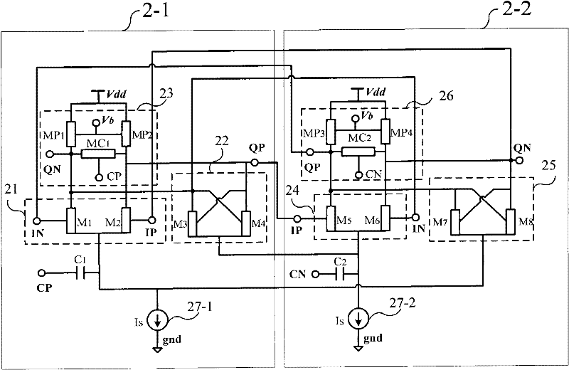
[0077] The tube-level schematic diagram of the basic circuit structure of the low-voltage high-speed frequency divider of the present invention is as follows: Figure 2a shown. The low-voltage high-speed divider consists of two identical latches 2-1 and 2-2 cross-coupled with clocked transistors. The first latch 2-1 with clocked transistors includes: a sampling differential pair amplifier 21 composed of M 1 and M 2 composed of a latched cross-coupled pair amplifier 22 consisting of M 3 and M 4 composed, as the load module 23 consists of the load tube M P1 ,M P2 and clock control tube M C1 composition. The second latch 2-2 with clocked transistors includes a sampling differential pair amplifier 24 composed of M 5 and M 6 composed of a latched cross-coupled pair amplifier 25 consisting of M 7 and M 8 composed, as the load module 26 consists of the load tube M P3 ,M P4 and clock control tube M C2 composition.
no. 2 Embodiment
[0079] For the tube-level structure composition diagram of another latch 2-1 with a low-voltage clocked transistor, see Figure 2b . The differential signals CN and CP from the front-end VCO or other devices are added to the drain of the tail current source after passing through the DC blocking capacitor, the differential signal CN is also connected to the source of the sampling differential pair 21, and the differential signal CP is also connected to The source of the differential pair transistor 22 is latched. The differential signal input terminals of the sampling differential pair tube 21 of the latch with clocked transistor 2-1 are IP and IN, the cross-coupled output terminals of the latch cross-coupled pair tube 22 are QP and QN, and the cross-coupled output terminals QP and QN is connected to the load module 23 clock control tube MC in parallel 1 source and drain of the load module 23 Z 1 and Z 2 is the load tube, load tube Z 1 ,Z 2 and clock control tube MC 1 Ca...
no. 3 Embodiment
[0081] Such as image 3 Shown is the composition circuit diagram of the low-voltage high-speed frequency divider of the third embodiment. The low-voltage high-speed frequency divider includes a first latch 3-1 and a second latch 3-2. The first latch consists of the M 1 and M 2 consists of 31 sampled differential pairs and consists of M 5 and M 6 Composed of 32 latched cross-coupled pairs, the MP 1 , MP 2 and clock control tube MC 1 The composed load module 33 also includes a first tail current source. The second latch consists of the M 5 and M 6 The sampling differential pair consists of tube 34, and consists of M 7 and M 8 composed of 35 latched cross-coupled pairs, consisting of MP 3 , MP 4 and clock control tube MC 2 Consisting of load module 36, also includes a second tail current source. image 3 , amplifier M 1 ~ M 8 All are NMOS tubes, the MP in the load module 1 ~MP 4 and clock control tube MC 1 ~MC 2 All are PMOS tubes. The clock signal CP passes ...
PUM
 Abstract
Description
Claims
Application Information
 - R&D
- Intellectual Property
- Life Sciences
- Materials
- Tech Scout
- Unparalleled Data Quality
- Higher Quality Content
- 60% Fewer Hallucinations
Browse by: Latest US Patents, China's latest patents, Technical Efficacy Thesaurus, Application Domain, Technology Topic, Popular Technical Reports.
© 2025 PatSnap. All rights reserved.Legal|Privacy policy|Modern Slavery Act Transparency Statement|Sitemap|About US| Contact US: help@patsnap.com