Microelectrode array with adjustable electrode point distance

A micro-electrode array and electrode technology, which is applied in the field of medical devices, can solve the problems of micro-electrode arrays with variable electrode point distances that have not been reported, and achieve the effect of simple structure and convenient use

Active Publication Date: 2015-01-21
SHANGHAI JIAO TONG UNIV
View PDF7 Cites 0 Cited by
  • Summary
  • Abstract
  • Description
  • Claims
  • Application Information

AI Technical Summary

Problems solved by technology

[0009] In summary, although the preparation method of the microelectrode array has been studied in detail, and the related extension function of the microelectrode array has also been paid attention to, but there is no microelectrode array with variable electrode point distance reported in the literature.

Method used


Image

  • Microelectrode array with adjustable electrode point distance

Examples


Embodiment 1

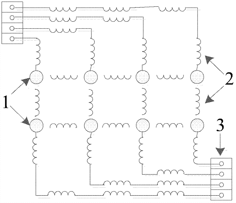
[0025] Such as figure 1 As shown, the microelectrode array described in this embodiment includes: a microelectrode array structure layer, an electrode circuit layer, and a microelectrode array covering layer, wherein: the electrode circuit layer is sandwiched between the microelectrode array structure layer and the microelectrode array covering layer . Considering that the three-layer structure of the microelectrode array has been described in detail in the patent (application number 201110110285.0, application publication number CN 102178998A), only the characteristics of the electrode circuit layer will be highlighted here.

[0026] In this embodiment, the electrode circuit layer includes electrode points 1 , a buffer structure 2 that facilitates adjustment of the distance between the electrode points, and connection points 3 with peripheral circuits.

[0027] In this embodiment, the distribution distance and distribution density of the buffer structures 2 in the electrode ...

Embodiment 2

[0044] This embodiment provides the preparation method of the microelectrode array described in Embodiment 1, and the specific process is as follows:

[0045] Firstly, 10 μm PDMS (polydimethylsiloxane) was cast on the Si wafer and cured to form a microelectrode structure layer;

[0046] Then throw a 5 μm positive resist and pattern it, sputter the noble metal (including Pt, Ir, Au, etc.) seed layer, 100-15000 angstroms, use the Lift-off process to remove the photoresist, pattern the seed layer, and form the electrode circuit layer;

[0047] Then throw 10μm PDMS (polydimethylsiloxane) and cure it, pattern the photoresist for the second time, and use reactive ion etching (RIE) to etch through Parylene-C to expose the electrode points to form a microelectrode Array overlay.

Embodiment 3

[0049] This embodiment provides the preparation method of the microelectrode array described in Embodiment 1. In this embodiment, polychlorinated p-xylylene (Parylene-C) is used for the microelectrode structure layer and the covering layer, and the preparation process is as follows:

[0050] First deposit a 5 μm polychlorinated p-xylylene (Parylene-C) film on the Si wafer, then throw a 5 μm positive resist and pattern it, and sputter a noble metal (including Pt, Ir, Au, etc.) seed layer, 100-15000 Angstroms, Use the Lift-off process to remove the photoresist, pattern the seed layer, and form the electrode circuit layer. Then deposit 5 μm of Parylene-C, pattern the photoresist for the second time, and use reactive ion etching (RIE) to etch through Parylene-C to expose electrode points to form a microelectrode array covering layer.

[0051] In summary, using the microelectrode array with adjustable electrode point spacing to collect and stimulate electrophysiological signals, co...


PUM

PropertyMeasurementUnit
radiusaaaaaaaaaa
areaaaaaaaaaaa
diameteraaaaaaaaaa

Abstract

The invention discloses a microelectrode array with an adjustable electrode point distance, comprising a microelectrode array structural layer, an electrode circuit layer and a microelectrode array covering layer which are sequentially arranged and form a composite structure, wherein the microelectrode array covering layer is directly contacted with a tissue, and electrode points and a buffer structure convenient for adjusting the electrode point distance are arranged in the electrode circuit layer. For the microelectrode array, the buffer structure formed by a series of small arcs is used for controlling the electrode point distance, when the small arcs are tensioned transversely or longitudinally, the radius of the small arc is increased, the radian is reduced, the electrode point distance is changed, and the damage of the circuit structure, caused by tensioning, is reduced to the minimum. In the traditional microelectrode array with the fixed distance, the microelectrode array only needs to be properly tensioned to obtain the microelectrode array with different distances in practical use, but multiple traditional microelectrode arrays with the fixed distances are needed to achieve the same effect.

Description

technical field [0001] The invention relates to a microelectrode array in the technical field of medical equipment, in particular to a microelectrode array with adjustable electrode point spacing for electrophysiological applications. Background technique [0002] In recent years, with the continuous advancement of micro-electro-mechanical systems (MEMS: Micro-Electro-Mechanical Systems) technology, the application range of micro-systems such as micro-electronic devices and micro-sensors has continued to expand, and has been widely used in many fields, especially in the medical field. . [0003] Microelectrode array is a typical application of MEMS technology in biomedicine. Microelectrode arrays are electrodes arranged in a dot matrix on the surface of the substrate. The diameter of common electrode points is 50-100 μm, and the distance between electrode points is 100-1000 μm. Simultaneous recording of extracellular field potential signals at multiple sites. Microelectro...

Claims


Application Information

Patent Timeline
Patent Type & Authority Patents(China)
IPC IPC(8): B81B1/00B81C1/00G01N27/00
Inventor 刘景全康晓洋田鸿昌杨春生
Owner SHANGHAI JIAO TONG UNIV
Why Eureka
Try Eureka