Check patentability & draft patents in minutes with Patsnap Eureka AI!

Solution and method for preparing nano-pore arrays on surfaces of silicon chip

A nanopore array, silicon wafer surface technology, applied in anodizing and other directions, can solve problems such as legal restrictions on development, and achieve the effect of improving conversion efficiency, simplifying processing procedures, and good environmental compatibility

Inactive Publication Date: 2012-07-11
HOHAI UNIV CHANGZHOU
View PDF3 Cites 0 Cited by
  • Summary
  • Abstract
  • Description
  • Claims
  • Application Information

AI Technical Summary

Problems solved by technology

Literature (Bohr-Ran Huang, Ying-KanYang, Tzu-ChingLin, Wen-LuhYang, A simple and low-cost technique for silicon nanowire arrays based solar cells, Solar Energy Materials & Solar Cells 98 (2012) 357–362.) and Documents (Priyamka Singh, Shailesh N. Sharmma and N. M. Ravindra, Applications of porous silicon thin films in Solar cells and biosensors, JOM, 26(6)(2010) 17-24.) respectively describe the use of HF acid-containing films on the surface of silicon wafers. Solution anodizing process for treating nanopores, but both use HF acid solution that affects the environment, and the development of this process will gradually be restricted by laws

Method used


Image

  • Solution and method for preparing nano-pore arrays on surfaces of silicon chip

Examples


Embodiment 1

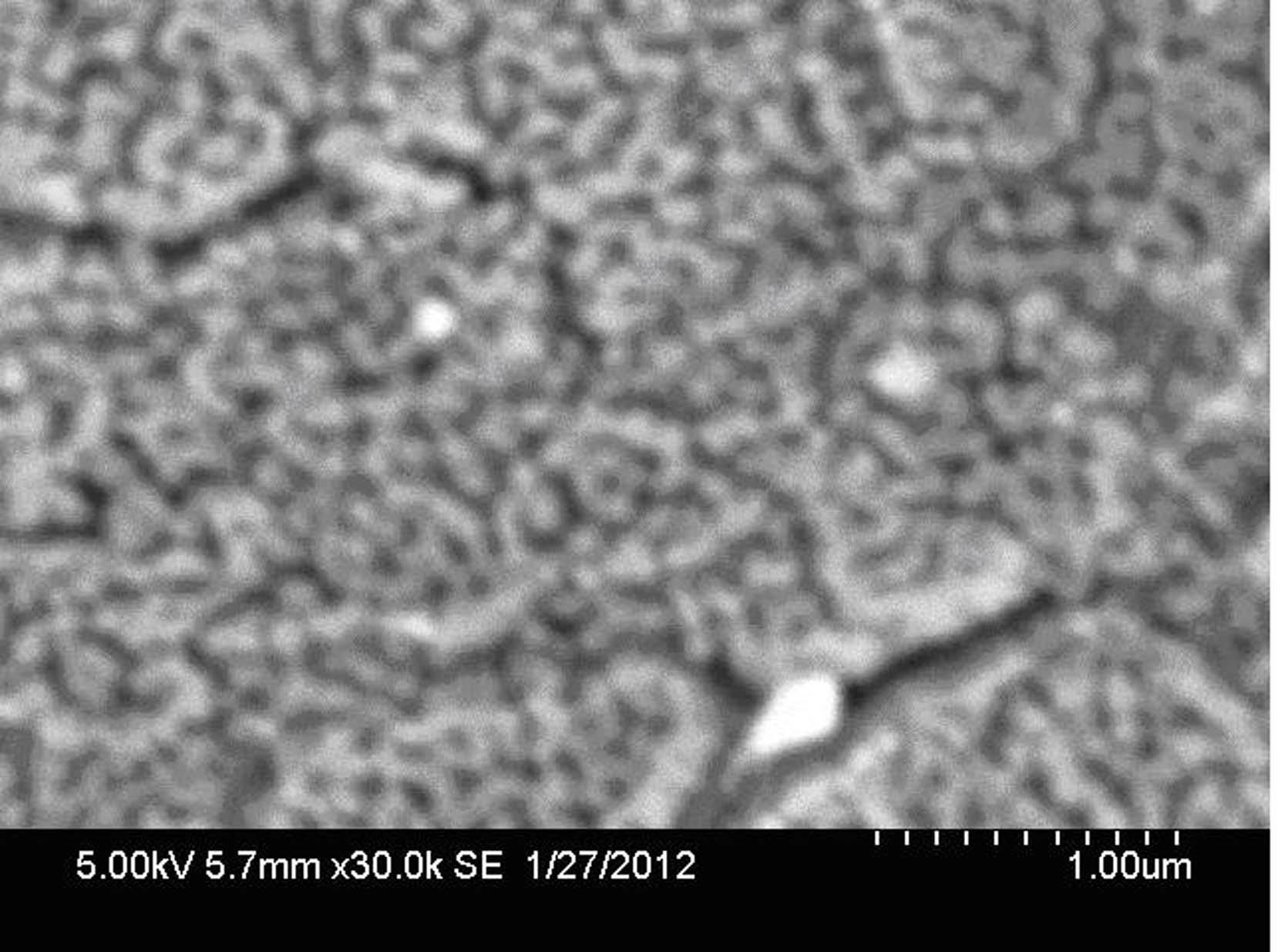
[0011] Embodiment 1: Add 56g oxalic acid, 44mL glycerin solution in 1L deionized water, take silicon chip as anode, stainless steel as cathode, process under 45V voltage for 4 hours, the aperture of its nanopore is less than 500nm, illustrate that processing can obviously reduce Wafer processing costs.

Embodiment 2

[0012] Example 2: First, take 2 / 3 of deionized water in a 10L tank, add 560g of oxalic acid and 810mL of glycerol in turn under stirring, and finally add water to 10L to obtain an electrolyte, with a silicon chip as the anode and a stainless steel as the cathode , treated at a voltage of 60V for 5 hours, the diameter of the nanopores is less than 800nm.

Embodiment 3

[0013] Embodiment 3: first take 2 / 3 deionized water in a 10L tank, add 700mL of phosphoric acid and 1200mL of ethanol with a concentration of 85% successively under stirring, finally add water to 10L, obtain electrolyte, use silicon chip as anode, The stainless steel is used as the cathode, and it is treated at 40V for 2 hours, and the diameter of the nanopores is less than 600nm.


PUM


Abstract

The invention discloses a solution and a method for preparing nano-pore arrays on the surfaces of a silicon chip. The method comprises the following steps of: putting the silicon chip into the solution which comprises the following components in percentage by weight: 5 to 10 percent of acid, 5 to 10 percent of organic alcohol and 80 to 85 percent of water, wherein the acid is oxalic acid or 85 percent phosphoric acid, the organic alcohol is ethanol or glycerol, and the water is deionized water; and treating at the voltage of 40 to 60V for 1 to 8 hours by taking the silicon chip as an anode and stainless steel or an inert electrode material as a cathode, and taking the silicon chip out to obtain the silicon chip with nano-pores on the two surfaces. A fluorine-free anodic oxidation technology process for the silicon chip is adopted, and the method is compatible with the environment and has the characteristic of environment friendliness; the solution is at room temperature, so that the process of treating the silicon chip is simplified; and the diameter, depth and distribution density of the nano-pores on the surfaces of the treated silicon chip can be adjusted according to the process, so that cost is reduced, and the conversion efficiency of light is improved.

Description

technical field [0001] The invention belongs to the technical field of silicon surface treatment, and in particular relates to a method for preparing a nanohole array through the fluorine-free anodic oxidation technology on the surface of a silicon chip, which is applicable to the field of solar photoelectric conversion. Background technique [0002] Silicon is a key material in the manufacture of solar cells. Since 30% of the incident light is reflected on the surface of the silicon wafer, attention has been paid to improving the light absorption and conversion capabilities of the silicon wafer surface. Anodizing the surface of silicon wafers to form nanopore arrays is one of the methods to solve the problem of light absorption and conversion. Literature (Bohr-Ran Huang, Ying-KanYang, Tzu-ChingLin, Wen-LuhYang, A simple and low-cost technique for silicon nanowire arrays based solar cells, Solar Energy Materials & Solar Cells 98 (2012) 357–362.) and Documents (Priyamka Sin...

Claims


Application Information

Patent Timeline
Patent Type & Authority Applications(China)
IPC IPC(8): C25D11/32
Inventor 蒋永锋包晔峰杨可
Owner HOHAI UNIV CHANGZHOU
Features
  • R&D
  • Intellectual Property
  • Life Sciences
  • Materials
  • Tech Scout
  • Unparalleled Data Quality
  • Higher Quality Content
  • 60% Fewer Hallucinations
Learn More