N-type czochralski silicon with uniform doping resistivity and preparation method thereof

A technology of Czochralski silicon and resistivity, applied in the field of solar cell materials, can solve the problems of low utilization rate of high-efficiency solar cell materials, large axial variation range of resistivity of N-type Czochralski silicon single crystal, etc., and achieve easy large-scale application , Improve the utilization rate, reduce the effect of manufacturing cost

Active Publication Date: 2012-07-11
ZHEJIANG UNIV
View PDF7 Cites 7 Cited by
  • Summary
  • Abstract
  • Description
  • Claims
  • Application Information

AI Technical Summary

Problems solved by technology

[0007] The invention provides a method for preparing N-type Czochralski silicon single crystal with uniform doping resistivity, which can control the resistivity of the entire N-type silicon single crystal within the range of 1.0-2.0Ω.cm, and solves the problem of N-type Czochralski silicon single crystal resistivity has a large axial variation range, and the problem of low utilization rate of high-efficiency solar cell materials

Method used


Image

  • N-type czochralski silicon with uniform doping resistivity and preparation method thereof
  • N-type czochralski silicon with uniform doping resistivity and preparation method thereof

Examples


Embodiment 1

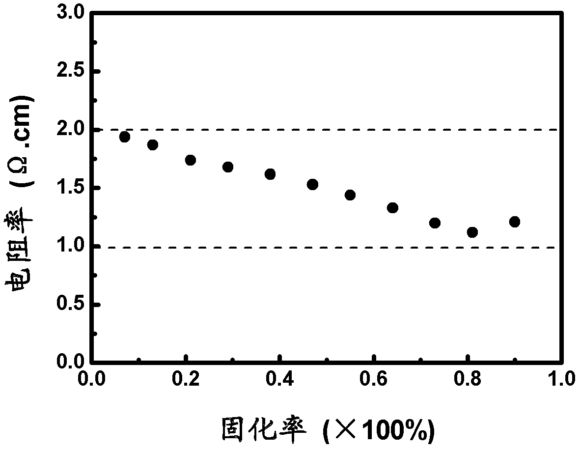
[0022] First put 11.05mg of phosphorus and 361.81mg of gallium into the bottom of the quartz crucible, then put 50kg of high-purity electronic grade polysilicon into the quartz crucible; under the protection of argon, melt the polysilicon at 1410°C to melt the phosphorus and gallium into the polysilicon In the solution, adjust the crystal growth parameters (pot rotation 10r / min, crystal rotation 20r / min, protective gas flow rate 100torr), and grow a Czochralski silicon single crystal with a diameter of 150mm at a growth rate of 1.2mm / min. Samples were taken at different parts of the grown crystal, and the axial distribution of the resistivity of the grown crystal was tested by the four-probe method, as shown in the attached figure 1 shown. It can be seen that the resistivity of the whole crystal is distributed between 1.0-2.0Ω.cm. As a result, the utilization of silicon material is increased by 22% relative to the crystal without gallium doping compensation. The efficiency o...

Embodiment 2

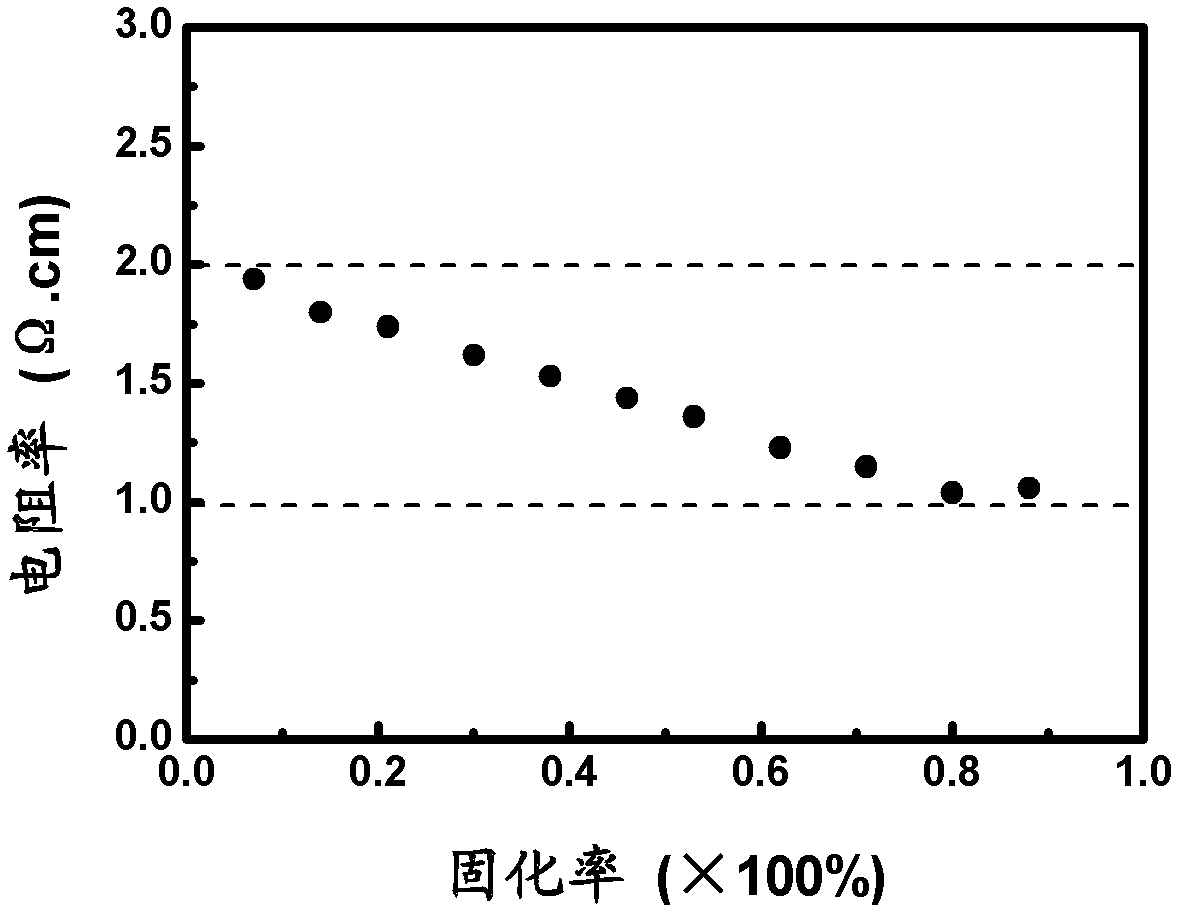
[0024] First put 9.47mg of phosphorus and 517.66mg of gallium into the bottom of the quartz crucible, and then put 50kg of metallurgical grade compensation silicon material (containing 0.49mg of boron and 6.31mg of phosphorus in total) into the quartz crucible; under the protection of argon , melt the polysilicon material at 1410°C, melt phosphorus and gallium into the polysilicon solution, adjust the crystal growth parameters (pot rotation 15r / min, crystal rotation 37r / min, protective gas flow rate 200torr), and grow at a growth rate of 1.5mm / min A Czochralski silicon single crystal with a diameter of 150 mm. Samples were taken at different parts of the grown crystal, and the axial distribution of the resistivity of the grown crystal was tested by the four-probe method, as shown in the attached figure 2 shown. It can be seen that the resistivity of the whole crystal is distributed between 1.0-2.0Ω.cm. As a result, the utilization of silicon material is increased by 30% rel...


PUM

PropertyMeasurementUnit
electrical resistivityaaaaaaaaaa

Abstract

The invention discloses an N-type czochralski silicon with a uniform doping resistivity and a preparation method thereof. The preparation method comprises the following steps of: mixing a polycrystalline silicon material, a phosphorus doping agent and gallium; fusing; and growing a silicon monocrystal by using a czochralski method. According to the N-type czochralski silicon with the uniform doping resistivity prepared by using the method, the resistivity of a whole crystal of the N-type czochralski silicon can be controlled in the range of 1.0-2.0 omega.cm, therefore, the utilization rate of the N-type silicon crystal in the process of manufacturing a solar cell is effectively improved, the manufacturing cost of the solar cell is remarkably lowered, the preparation method is simple to operate and easy to popularize and use in the photovoltaic industry.

Description

technical field [0001] The invention belongs to the field of solar cell materials, in particular to an N-type Czochralski silicon single crystal with uniform doping resistivity and a preparation method thereof. Background technique [0002] Solar energy is an inexhaustible and inexhaustible clean energy. Using the photoelectric conversion characteristics of semiconductor materials, it can be prepared into solar cells, which can convert solar energy into electrical energy. In the last ten years, the output of solar cells has grown at an annual rate of 30-40%, and the solar industry has become one of the fastest growing industries in the market today. [0003] Czochralski silicon single crystal is one of the main materials for preparing solar cells. In traditional solar photovoltaic technology, boron-doped p-type silicon single crystal is widely used in the preparation of solar cells. However, under light, the boron-doped P-type silicon single crystal will lead to a signific...

Claims


Application Information

Patent Timeline
Patent Type & Authority Applications(China)
IPC IPC(8): C30B15/04C30B29/06
Inventor 余学功肖承全杨德仁
Owner ZHEJIANG UNIV
Why Eureka
Try Eureka