Method for manufacturing planar high-voltage ultrafast soft recovery diode

A technology for recovering diodes and a manufacturing method, which is applied in semiconductor/solid-state device manufacturing, electrical components, circuits, etc., can solve the problems of unsuitable large-scale industrial production, high price of epitaxial silicon materials, and expensive epitaxial materials, etc. Reverse recovery characteristics, low cost, and the effect of speeding up extraction

Active Publication Date: 2012-07-11
BEIJING MXTRONICS CORP +1
View PDF3 Cites 37 Cited by
  • Summary
  • Abstract
  • Description
  • Claims
  • Application Information

AI Technical Summary

Problems solved by technology

However, the disadvantage of this manufacturing method is that the price of the epitaxial silicon material is high, and the cost of the product is increased. It is generally manufactured as a fast recovery diode below 1200V. For devices above 1200V, the thickness of the high-resistance layer is above 160um. Reach the limit of the current epitaxial level, and this type of epitaxial material is expensive, not suitable for large-scale industrial production
Therefore, the epitaxial process technology is not suitable for the production and manufacture of high voltage (above 1200V) fast recovery diodes

Method used


Image

  • Method for manufacturing planar high-voltage ultrafast soft recovery diode
  • Method for manufacturing planar high-voltage ultrafast soft recovery diode
  • Method for manufacturing planar high-voltage ultrafast soft recovery diode

Examples


Embodiment Construction

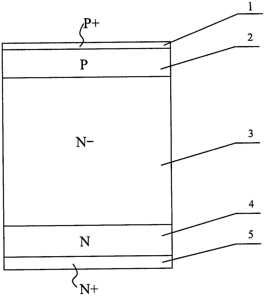
[0040] Such as image 3 As shown, the vertical structure adopted by the present invention is composed of an anode contact P+ layer 1, an anode region P type layer 2, an N- high resistance layer 3, an N type buffer layer 4, and a cathode contact N+ layer 5. The horizontal terminal structure adopted is such as Figure 4 As shown, it includes a field limiting ring 9, a polysilicon field plate 7 and an N+ type stop ring 10. One end of the polysilicon field plate 7 is in contact with the field limiting ring 9, and the other end is under the initial oxide layer 8, and the passivation layer 6 covers the entire terminal. .

[0041] The longitudinal structure of the chip adopts the P+PN-NN+ structure, such as image 3 As shown, the P+ layer 1 and the N+ layer 5 are the contact layers of the anode and the cathode respectively, which form a good ohmic contact with the metal electrode and reduce the forward voltage drop; the P-type layer 2 in the anode region adopts the anode emission efficie...


PUM

PropertyMeasurementUnit
electrical resistivityaaaaaaaaaa

Abstract

The invention discloses a method for manufacturing a planar high-voltage ultrafast soft recovery diode. The method comprises the following steps of: oxidizing, and photoetching to form an active region and a field limiting ring; doping and pushing; manufacturing a polycrystalline silicon field plate; performing platinum diffusion; thinning; forming an N-type buffer layer; performing contact doping and annealing; and metalizing. The method can be used for manufacturing an ultrafast soft recovery diode chip which is low in cost and short in recovery time and has high-voltage resistance, low leakage current, low forward voltage drop and soft recovery characteristics.

Description

Technical field [0001] The invention relates to the field of power semiconductor devices, in particular to a method for manufacturing a planar high-voltage ultra-fast soft recovery diode. Background technique [0002] As the core device in power electronic circuits, power semiconductor devices are used to achieve high-efficiency transmission and conversion of electrical energy and effective and precise control in the process, so as to achieve high-quality and efficient use of electrical energy. It is precisely because of the research and development of power semiconductor devices that power electronic technology is developing in the direction of large capacity, high frequency, high efficiency and energy saving, high reliability and low cost. Fast Recovery Diode (FRD) is a new type of power device that has come out in recent years. It has the advantages of good switching performance, short reverse recovery time, large forward current, small size, and easy installation. It is widel...

Claims


Application Information

Patent Timeline
Patent Type & Authority Applications(China)
IPC IPC(8): H01L21/329
Inventor 王成杰王传敏殷丽冯幼明刘军姚全斌郭晨光
Owner BEIJING MXTRONICS CORP
Why Eureka
Try Eureka