

Method of fabricating array substrate for liquid crystal display
A liquid crystal display and array substrate technology, applied in the field of etchant compositions, can solve problems such as inability to meet user needs, and achieve the effects of realizing large-size screens, preventing short circuits, and excellent etching uniformity
Active Publication Date: 2012-07-11
DONGWOO FINE CHEM CO LTD
View PDF6 Cites 10 Cited by
- Summary
- Abstract
- Description
- Claims
- Application Information
AI Technical Summary
Problems solved by technology
However, because the performance of the etchant compositions known so far for copper-based metal layers cannot meet the needs of users, research and development to improve this performance is underway.
Method used
View moreImage
Smart ImageViewing Examples

Examples
Embodiment 1~12
[0041] Embodiments 1-12: Etchant composition for preparing Cu-based metal layer
[0042] The ingredients of the etchant compositions prepared in Examples 1-12 are shown in Table 1 below.
[0043] Table 1
[0044]
[0045] * HEDP: 1-Hydroxyethylidene-1,1-diphosphonic acid
Login to View More PUM
 Abstract
Disclosed is a method of fabricating an array substrate for a liquid crystal display, including forming a copper-based metal layer on a substrate and etching the copper-based metal layer using an etchant composition thus forming gate wiring, and forming a copper-based metal layer on a semiconductor layer and etching the copper-based metal layer using the etchant composition thus forming source / drain electrodes, the etchant composition including based on the total weight of the composition, A) 5.0 ~ 25 wt% of hydrogen peroxide (H2O2), B) 0.01 ~ 1.0 wt% of a fluorine-containing compound, C) 0.1 ~ 5.0 wt% of an azole compound, D) 0.1 ~ 10.0 wt% of one or more compounds selected from among phosphonic acid derivatives and salts thereof, and E) a remainder of water.
Description
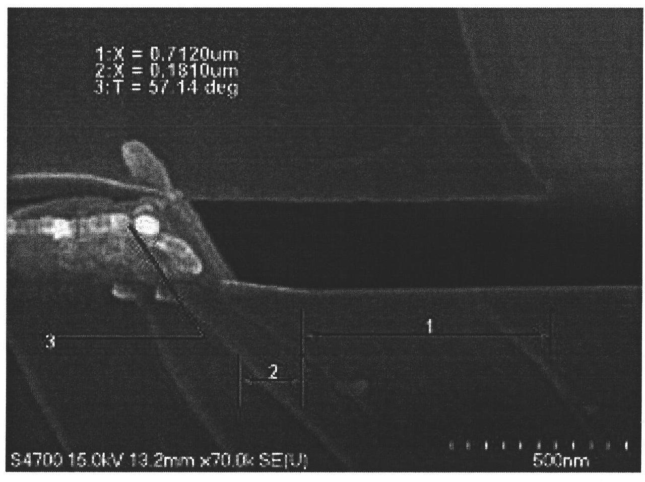
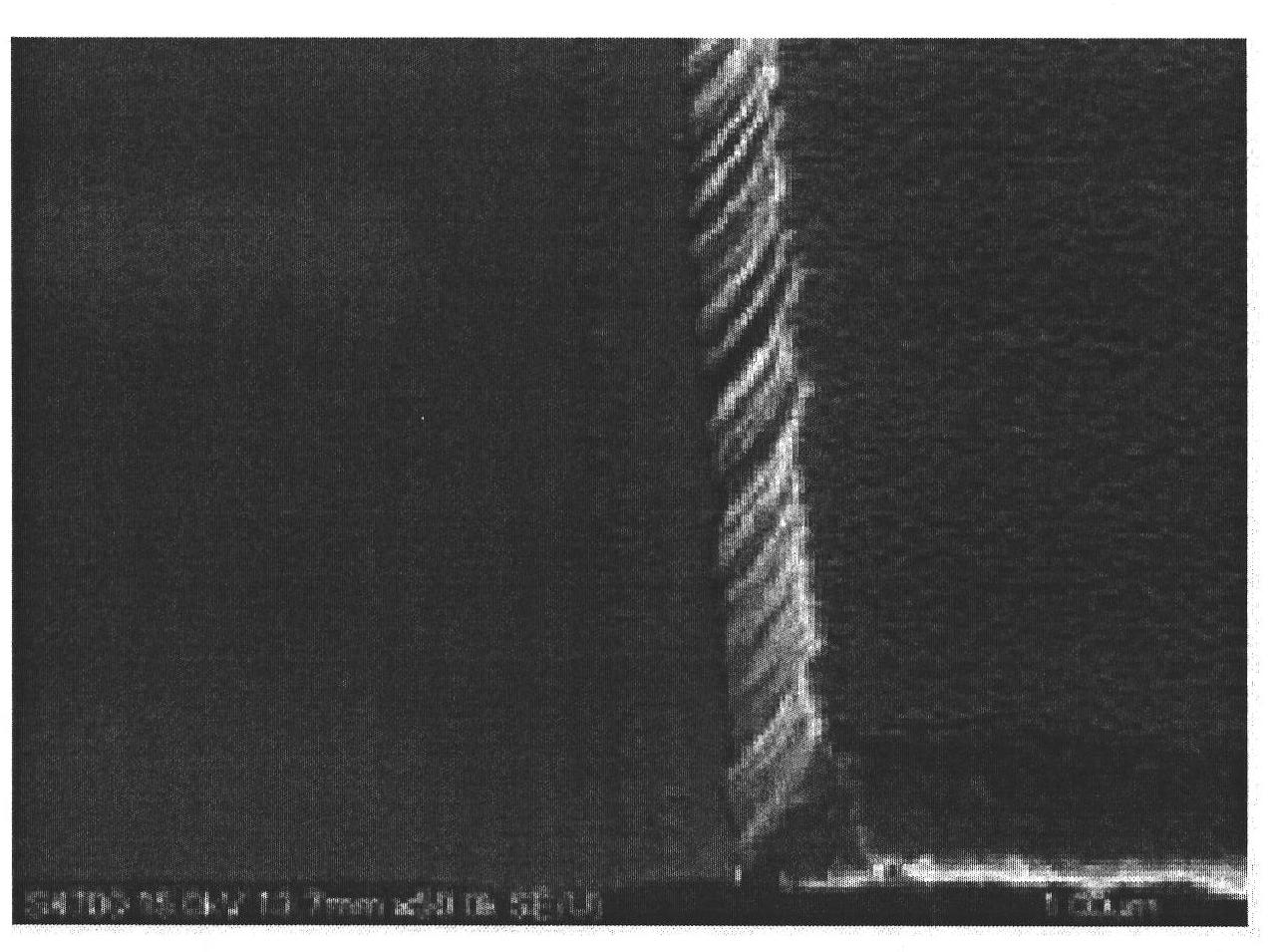
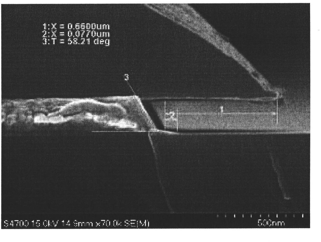
technical field [0001] The invention relates to a method for manufacturing an array substrate for a liquid crystal display, an etchant composition for a copper-based metal layer, and a method for etching a copper-based metal layer using the etchant composition. Background technique [0002] In general, forming metal wiring on a substrate of a semiconductor device includes forming a metal layer by sputtering, coating a photoresist, performing exposure and development so that the photoresist is formed on a selected area, and performing etching, and A cleaning process is performed before or after each individual process. During the etching process, the metal layer is formed on selected areas using the photoresist as a mask. The etching process generally includes dry etching using plasma or wet etching using an etchant composition. [0003] Recently, in such semiconductor devices, the resistance of metal wiring is considered to be very important. This is because resistance is...
Claims
Login to View More Application Information
Patent Timeline
 IPC IPC(8): G02F1/136
CPCH01L27/1214H01L27/124
Inventor李铉奎李友兰郑敬燮崔容硕李石尹暎晋
OwnerDONGWOO FINE CHEM CO LTD