

P-type heavily-doped silicon carbide film extension preparation method
A technology of silicon carbide and heavy doping, which is applied in semiconductor/solid-state device manufacturing, electrical components, circuits, etc., to achieve the effect of satisfying heavy doping of devices, high doping concentration, and improving device performance
- Summary
- Abstract
- Description
- Claims
- Application Information
AI Technical Summary
Problems solved by technology
Method used
Image

Examples
Embodiment 1
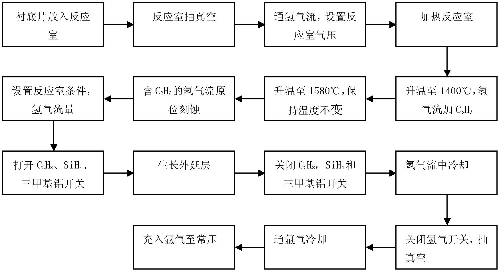
[0034] Step 1, placing the silicon carbide substrate into the reaction chamber of the silicon carbide CVD equipment.
[0035] (1.1) Selection bias A 4H silicon carbide substrate with a crystal orientation of 8° is placed in the reaction chamber of the silicon carbide CVD equipment;
[0036] (1.2) Vacuumize the reaction chamber until the pressure in the reaction chamber is lower than 1×10 -7 mbar.
[0037] Step 2, heating the reaction chamber in the hydrogen flow.
[0038] (2.1) Open the hydrogen switch leading to the reaction chamber, and control the hydrogen flow to gradually increase to 20L / min;
[0039] (2.2) Turn on the vacuum pump to extract the gas in the reaction chamber, and keep the pressure in the reaction chamber at 100mbar;
[0040] (2.3) Gradually increase the power of the heating source to slowly increase the temperature of the reaction chamber.
[0041] Step 3, performing in-situ etching on the substrate.
[0042] (3.1) When the reaction chamber temperature...
Embodiment 2
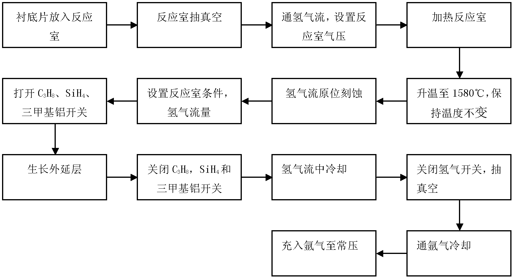
[0057] Step 1, select the direction The 4H silicon carbide substrate with a crystal orientation of 8° is placed in the reaction chamber of the silicon carbide CVD equipment; the reaction chamber is evacuated until the pressure of the reaction chamber is lower than 1×10 -7 mbar.
[0058] Step 2, turn on the hydrogen switch leading to the reaction chamber, control the hydrogen flow to gradually increase to 20L / min, and at the same time turn on the vacuum pump to extract the gas in the reaction chamber, keeping the pressure of the reaction chamber at 100mbar; gradually increase the power of the heating source to make the reaction chamber temperature Slowly increase, when the temperature of the reaction chamber is higher than 1400°C, add C with a flow rate of 7mL / min in the hydrogen flow 3 h 8 .
[0059] Step 3, when the temperature of the reaction chamber reaches 1580°C, keep the temperature of the reaction chamber constant, continue to feed hydrogen gas with a flow rate of 2...
Embodiment 3
[0064] In the first step, the silicon carbide substrate is placed in the reaction chamber of the silicon carbide CVD equipment.
[0065] (1.1) Selection bias A 4H silicon carbide substrate with a crystal orientation of 4° is placed in the reaction chamber of the silicon carbide CVD equipment;
[0066] (1.2) Vacuumize the reaction chamber until the pressure in the reaction chamber is lower than 1×10 -7 mbar.
[0067] In the second step, the reaction chamber is heated in a hydrogen flow.
[0068] (2.1) Open the hydrogen switch leading to the reaction chamber, and control the hydrogen flow to gradually increase to 20L / min;
[0069] (2.2) Turn on the vacuum pump to extract the gas in the reaction chamber, and keep the pressure in the reaction chamber at 100mbar;
[0070] (2.3) Gradually increase the power of the heating source to slowly increase the temperature of the reaction chamber. When the temperature of the reaction chamber is higher than 1400°C, add C with a flow rate ...
PUM
 Abstract
Description
Claims
Application Information