

Preparation method for highly-doped phosphorosilicate glass film
A high-doping technology of phosphosilicate glass, applied in semiconductor/solid-state device manufacturing, gaseous chemical plating, coating, etc., can solve the problems of low starting point at the bottom of flower-shaped shell, device damage, low switching point, etc., to achieve Effects of protection from damage, maintenance performance, and uniform phosphorus doping amount
- Summary
- Abstract
- Description
- Claims
- Application Information
AI Technical Summary
Problems solved by technology
Method used
Image

Examples
Embodiment Construction
[0026] In order to have a more specific understanding of the technical content, characteristics and effects of the present invention, now in conjunction with the illustrated embodiment, the details are as follows:
[0027] The invention provides a method for preparing a highly doped phosphosilicate glass film. The method adopts two different steps of sub-atmospheric pressure chemical vapor deposition (SACVD) and high-density plasma chemical vapor deposition (HDP CVD). Highly doped phosphosilicate glass is grown by the deposition process, and the specific steps are as follows:
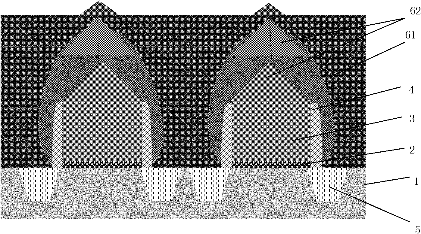
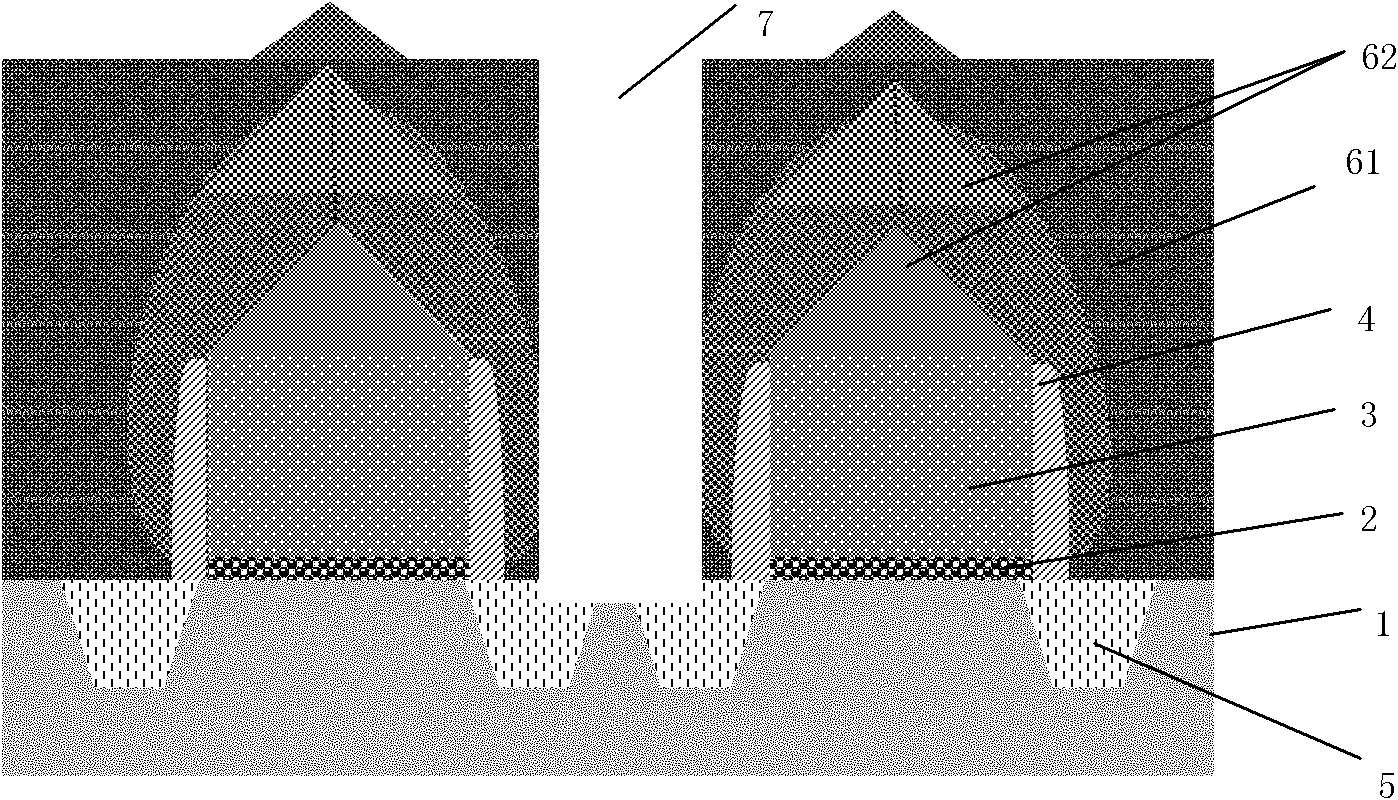
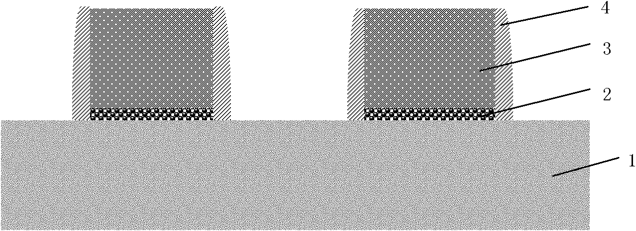
[0028] Step 1, please refer to Figure 3A A gate oxide layer 2 is grown on a silicon substrate 1 by using an existing process, and a polysilicon gate 3 and sidewalls 4 are prepared.
[0029] Step 2, please refer to Figure 3B , on the basis of the first step, performing drain-source implantation and rapid thermal annealing to form source and drain electrodes 5 .
[0030] Step 3, please refer to Fig...
PUM
 Abstract
Description
Claims
Application Information