Supercharge Your Innovation With Domain-Expert AI Agents!

Dielectric substrate and microstrip patch antenna using the same

A technology of microstrip patch antenna and dielectric substrate, which is applied in the directions of antenna, antenna support/installation device, radiating element structure, etc., can solve the problems of downsizing and the electrical performance of microstrip patch antenna, and improve the electromagnetic loss. , to achieve the effect of miniaturization

Active Publication Date: 2015-07-01
KUANG CHI INST OF ADVANCED TECH
View PDF6 Cites 0 Cited by
  • Summary
  • Abstract
  • Description
  • Claims
  • Application Information

AI Technical Summary

Problems solved by technology

When the dielectric constant of the dielectric substrate is increased by N times, the relationship between the wavelength and the dielectric constant is: The wavelength entering the dielectric substrate is the original The size of the microstrip patch antenna can also be reduced to the original Therefore, increasing the dielectric constant of the dielectric substrate is conducive to the miniaturization of the microstrip patch antenna, but the electromagnetic loss is usually greatly increased after the dielectric constant is increased, so that the electrical performance of the microstrip patch antenna is significantly reduced.

Method used


Image

  • Dielectric substrate and microstrip patch antenna using the same
  • Dielectric substrate and microstrip patch antenna using the same
  • Dielectric substrate and microstrip patch antenna using the same

Examples


Embodiment Construction

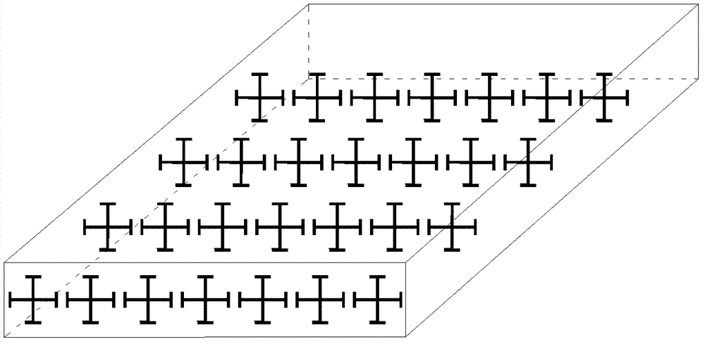
[0028] This embodiment provides a dielectric substrate, including a sheet of artificial electromagnetic material, of course, may also include a plurality of sheets of artificial electromagnetic material, when there are multiple sheets of artificial electromagnetic material, adjacent artificial electromagnetic material sheets are perpendicular to the The direction of the upper and lower surfaces can be assembled into one by mechanical connection, welding, or filling the material that can connect the two between adjacent artificial electromagnetic material sheets, such as Figure 5 The shown dielectric substrate comprises two artificial electromagnetic material sheets 1 and 2 bonded together by an adhesive layer 3 .

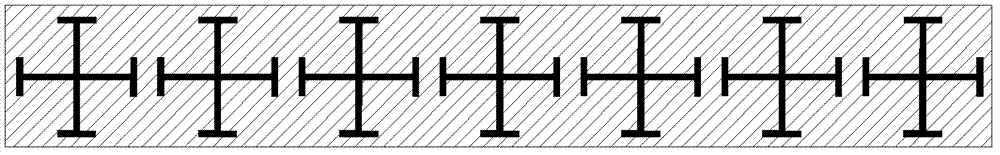
[0029] Such as figure 2 As shown, the artificial electromagnetic material sheet in this embodiment includes a substrate and a plurality of artificial microstructures arranged in an array attached to the side of the substrate and embedded in the substrate. When th...


PUM


Abstract

The invention relates to a dielectric substrate comprising at least one artificial electromagnetic material lamella. Each artificial electromagnetic material lamella comprises a substrate and at least two artificial microstructures attached at the side of the substrate or embedded at the inner part of the substrate. The artificial microstructures are in parallel to the direction of a preset electric field. The dielectric substrate has a higher dielectric constant. The invention also discloses a microstrip patch antenna using the dielectric substrate. The higher dielectric constant of the dielectric substrate is beneficial to realizing the miniaturization of the microstrip patch antenna.

Description

technical field [0001] The invention relates to a new material, more specifically, to a dielectric substrate and a microstrip patch antenna using the dielectric substrate. Background technique [0002] Artificial electromagnetic material is a new type of artificial synthetic material that can respond to electromagnetic waves. It consists of a substrate and an artificial microstructure attached to the substrate. Since the artificial microstructure is usually a structure with a certain geometric pattern composed of conductive materials, it can respond to electromagnetic waves, so that the artificial electromagnetic material as a whole exhibits electromagnetic properties different from that of the substrate. [0003] The dielectric constant is the ratio of the capacitance of a capacitor of the same size made of an insulating material as a medium to that of a capacitor of the same size made of a vacuum. It represents the amount of electrostatic energy accumulated in a unit volum...

Claims


Application Information

Patent Timeline
Patent Type & Authority Patents(China)
IPC IPC(8): H01Q1/12H01Q1/38H01Q13/08
Inventor 刘若鹏栾琳周添尹小明
Owner KUANG CHI INST OF ADVANCED TECH
Features
  • R&D
  • Intellectual Property
  • Life Sciences
  • Materials
  • Tech Scout
  • Unparalleled Data Quality
  • Higher Quality Content
  • 60% Fewer Hallucinations
Learn More