High-efficiency vertical cavity surface emitting semiconductor laser with asymmetric optical field distribution

A technology of vertical cavity surface emission and light field distribution, which is applied in the direction of semiconductor lasers, lasers, laser components, etc., can solve the problems of high loss, laser conversion efficiency limitation, etc., to increase output power, improve optical loss, and improve conversion efficiency Effect

Active Publication Date: 2012-07-25
SUZHOU EVERBRIGHT PHOTONICS CO LTD
View PDF6 Cites 11 Cited by
  • Summary
  • Abstract
  • Description
  • Claims
  • Application Information

AI Technical Summary

Problems solved by technology

[0005] The purpose of the present invention is to solve the problems of the high loss of the optical field of the existing vertical cavity surface emitting semiconductor laser on the side of the P-type DBR and the limitation of the conversion efficiency of the laser

Method used


Image

  • High-efficiency vertical cavity surface emitting semiconductor laser with asymmetric optical field distribution
  • High-efficiency vertical cavity surface emitting semiconductor laser with asymmetric optical field distribution
  • High-efficiency vertical cavity surface emitting semiconductor laser with asymmetric optical field distribution

Examples


Embodiment 1

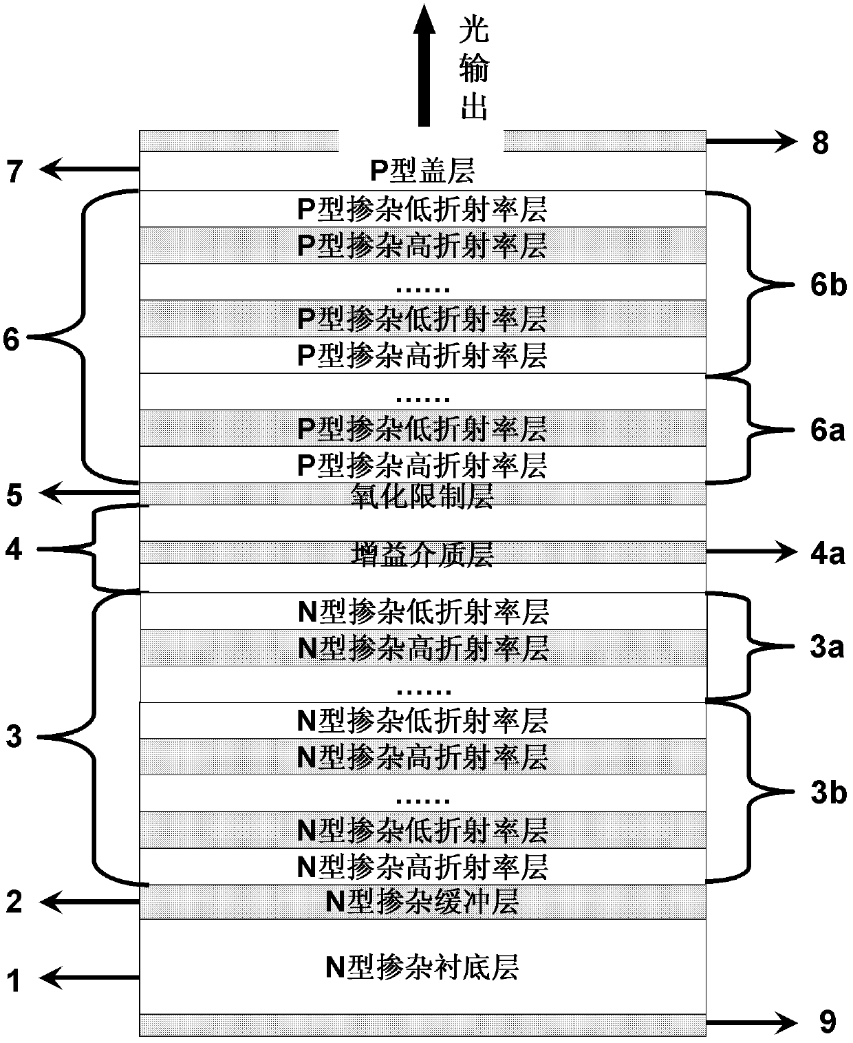
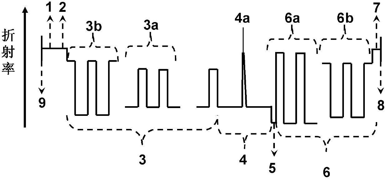
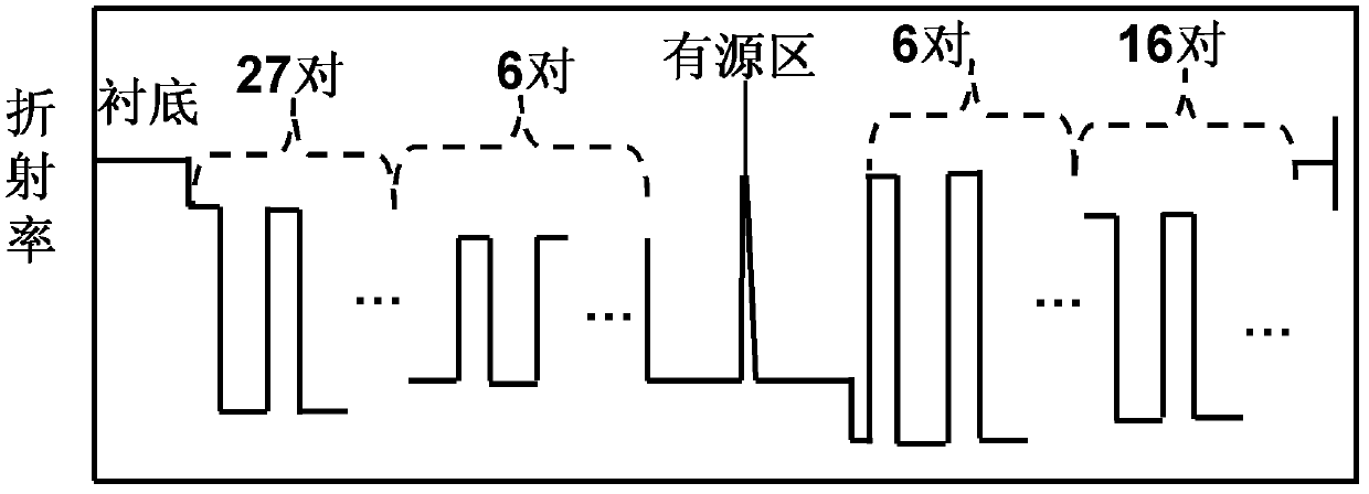
[0024] like Figure 3(a) , 3(b) , 3(c) shows the refractive index distribution, standing wave field distribution, and the relationship between output power and injection current of a vertical cavity surface emitting semiconductor laser with top-emitting asymmetric optical field distribution. In this structure, the total number of periodic material pairs of N-type segmented DBR3 is 33 pairs, and the total number of periodic material pairs of P-type segmented DBR6 is 22 pairs. The first 6 pairs of N-type DBRs and P-type DBRs close to the active area use low-refractive-index-difference and high-refractive-index-difference periodic materials, respectively. It can be seen from the distribution of the internal light field intensity of the device in Fig. 3 (b), that the distribution of the standing wave field inside the surface-emitting laser in the present invention is stronger than that of the P-type segment DBR6, that is, the light field is One side of the N-type segmented DBR3 ...

Embodiment 2

[0026] like Figure 4 As shown, compared with Embodiment 1, multiple periodic gain medium structures 4a, 4b and 4c are introduced into the active region 4 in this structure, and this structure can make the optical field obtain a large gain when it oscillates internally, thus obtaining High output power. The characteristic of this structure is that the thickness of the active region 4 is very large, and the standing wave field has multiple oscillation peaks inside the active region 4, and the gain medium is inserted at each corresponding peak position, which improves the utilization efficiency of the gain medium layer for the injected current , and the optical gain of the whole structure is greatly enhanced, thereby further increasing the optical power.


PUM


Abstract

In order to solve the problems of high optical field loss on P-type DBR (distributed Bragg reflector) side and restricted conversion efficiency of the existing vertical cavity surface emitting semiconductor laser, the invention relates to a high-efficiency vertical cavity surface emitting semiconductor laser with asymmetric optical field distribution, which belongs to the technical field of semiconductor laser. The high-efficiency vertical cavity surface emitting semiconductor laser with asymmetric optical field distribution comprises, from bottom to top, an N-side electrode, an N-type substrate, an N-type buffer layer, an N-type segmented DBR, an active region, an oxidation confinement layer, a P-type segmented DBR, a P-type cover layer and a P-side electrode, wherein the refractive index difference of the former 6 to 8 pairs of high- and low-refractive index material of the N-type segmented DBR close to the active region is smaller than that of the latter low-refractive index material pairs; and the refractive index difference of the former 6 to 8 pairs of high- and low-refractive index material of the P-type segmented DBR close to the active region is larger than that of the latter low-refractive index material pairs. The high-efficiency vertical cavity surface emitting semiconductor laser provided by the invention has high photoelectrical conversion efficiency, and wide application prospect.

Description

technical field [0001] The invention belongs to the technical field of semiconductor lasers, and in particular relates to a vertical cavity surface-emitting semiconductor laser with high-efficiency asymmetric light field distribution. Background technique [0002] Vertical cavity surface emitting laser is a semiconductor laser that emits light vertically on the surface. It has the advantages of low threshold, small divergence angle, high laser power density, easy monolithic integration, and good thermal stability. It is widely used in medical, sensing, display technology, There are extremely important applications in information storage, space communication and satellite navigation. With the expansion of application fields, the requirements for the performance of surface-emitting lasers are getting higher and higher. How to improve the efficiency of vertical-cavity surface-emitting semiconductor lasers has become a research hotspot in recent years. [0003] The existing ver...

Claims


Application Information

Patent Timeline
Patent Type & Authority Applications(China)
IPC IPC(8): H01S5/183H01S5/323
Inventor 张建伟宁永强秦莉刘云曾玉刚王立军
Owner SUZHOU EVERBRIGHT PHOTONICS CO LTD
Why Eureka
Try Eureka