
Thin film electroluminescence device and manufacturing method thereof

An electroluminescent device and thin film technology, applied in electroluminescent light sources, electric light sources, electrical components, etc., can solve problems such as restricting the development of color TFEL display devices, and achieve the effects of low cost, improved luminous efficiency, and simple manufacturing process

Inactive Publication Date: 2012-07-25
SOUTHEAST UNIV
View PDF2 Cites 10 Cited by
  • Summary
  • Abstract
  • Description
  • Claims
  • Application Information

AI Technical Summary

Problems solved by technology

Although Ifire is based on BaAl 2 S 4 :Eu blue light materials have successfully prepared electroluminescent displays, but blue TFEL devices have always restricted the development of color TFEL display devices

Method used


Image

  • Thin film electroluminescence device and manufacturing method thereof
  • Thin film electroluminescence device and manufacturing method thereof
  • Thin film electroluminescence device and manufacturing method thereof

Examples


Embodiment Construction

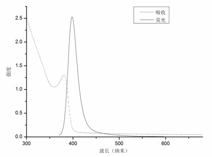
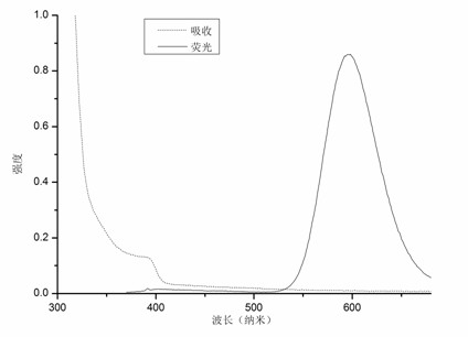
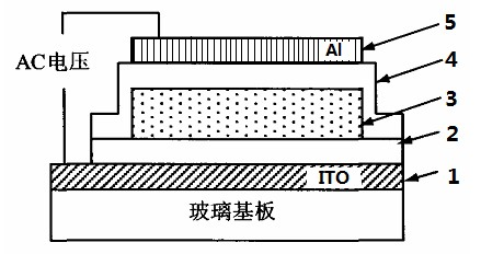
[0023] The light-emitting device includes an ITO conductive glass layer, a first insulating layer, a light-emitting layer, a second insulating layer and a metal electrode layer arranged in sequence, and the light-emitting layer is SiO2 gel-coated doped semiconductor quantum dots ZnSe:Mn / ZnS film.

[0024] The preparation of this device includes the following steps:

[0025] 1. Preparation of doped semiconductor quantum dots ZnSe:Mn / ZnS

[0026] ZnSe:Mn / ZnS was synthesized by growth-doping method. First, the Zn precursor ZnSt2 and ODE were stirred and degassed for 15 minutes in an Ar gas environment in a three-necked flask, and the Se precursor was injected at 270 ° C for 20 minutes, and the ZnSe quantum dots were obtained after purification and centrifugation. Take a certain amount of ZnSe quantum dots, oleylamine and ODE in a 50ml three-necked flask, and heat the degassed mixture to 120°C. Inject the MnSt2 / ODE reaction at this temperature for 5 min. After the temperature ...


PUM

PropertyMeasurementUnit
Thicknessaaaaaaaaaa

Abstract

The invention relates to a manufacturing method of a thin film electroluminescence device with doped semiconductor quantum dots being cladded with silica gel. The thin film electroluminescence device comprises an ITO (Indium Tin Oxide) conductive glass layer, a first insulating layer, a light emitting layer, a second insulating layer and a metal Al electrode which are arranged in sequence. The light emitting layer is formed by cladding doped semiconductor quantum dots with SiO2 gel; because the light emitting layer is prepared by cladding the doped semiconductor quantum dots with the silica gel, the compact degree of the light emitting layer can be improved, the breakdown resistance capability of the light emitting layer is effectively enhanced, the service life of the thin film electroluminescence device is prolonged, and the light emitting efficiency is improved. Meanwhile, in the thin film electroluminescence device of which the light emitting layer is prepared by cladding the doped semiconductor quantum dots with the silica gel, the thickness of the light emitting layer can be controlled relatively easily. Meanwhile, the manufacturing method disclosed by the invention can realize thin film electroluminescence devices with different light emitting intensities. The invention further provides the manufacturing method of the thin film electroluminescence device.

Description

technical field [0001] The invention relates to a thin-film electroluminescent device with silica gel-coated doped semiconductor quantum dots as a light-emitting layer and a preparation method thereof, belonging to the technical field of thin-film electroluminescent device manufacture. Background technique [0002] Currently, the three main flat panel display technologies are liquid crystal (LCD), plasma (PD) and AC thin film electroluminescent display (ACTFELD), which have their own advantages and disadvantages. ACTFELD has developed rapidly in recent years due to its advantages of fully solid-state flat panel display, active light emission, large viewing angle and wide temperature range, and has been widely used in scientific instruments and equipment, portable microcomputers, aerospace and military fields. Compared with liquid crystal display (LCD), thin-film electroluminescent display (TFEL) has the advantages of no backlight, high luminous intensity, and fast response s...

Claims


Application Information

Patent Timeline
IPC IPC(8): H05B33/14H05B33/10
Inventor 张家雨马骏杨伯平崔一平
Owner SOUTHEAST UNIV
Learn More