Preparation method of ohmic contact of metal with graphene

An ohmic contact and graphene technology, applied in semiconductor/solid-state device manufacturing, semiconductor devices, electrical components, etc., can solve problems such as obstruction, large contact resistance of field effect transistors, affecting device performance, etc., and achieve the effect of small contact resistance

Inactive Publication Date: 2012-08-01
INST OF MICROELECTRONICS CHINESE ACAD OF SCI
View PDF2 Cites 28 Cited by
  • Summary
  • Abstract
  • Description
  • Claims
  • Application Information

AI Technical Summary

Problems solved by technology

However, the further improvement of the performance of the graphene field effect tube has been greatly hindered. The contact resistance of the field effect tube is too large, and the

Method used


Image

  • Preparation method of ohmic contact of metal with graphene
  • Preparation method of ohmic contact of metal with graphene
  • Preparation method of ohmic contact of metal with graphene

Examples


Embodiment Construction

[0024] In order to make the object, technical solution and advantages of the present invention clearer, the present invention will be described in further detail below in conjunction with specific embodiments and with reference to the accompanying drawings.

[0025] The invention provides a method for preparing ohmic contact between metal and graphene, which is to use optical lithography or electron beam direct writing to realize device graphics on the graphene film, and irradiate the graphene in the contact area with oxygen ultraviolet rays or oxygen plasma. Part of the carbon atoms in the graphene in the contact area fall off, and finally the metal is evaporated to realize the ohmic contact between the metal and the graphene.

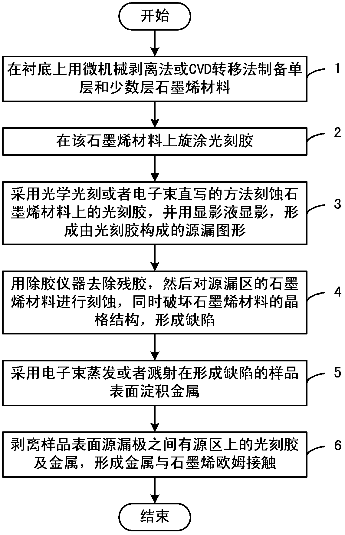
[0026] Such as figure 1 as shown, figure 1 It is a flow chart of a method for preparing metal and graphene ohmic contact according to an embodiment of the present invention, and the method includes the following steps:

[0027] Step 1: Prepare singl...


PUM


Abstract

The invention discloses a preparation method of ohmic contact of metal with graphene. The method includes preparing monolayer and a plurality of layers of graphene materials on a substrate through a micromechanical cleavage or a chemical vapor deposition (CVD) transferring method; spin-coating photoresist on the graphene materials; etching the photoresist on the graphene materials through optical lithography or an electron beam direct writing method, using a developer solution for development to form a source-drain image formed by the photoresist; removing residual gum with a degumming device, etching the graphene materials in a source-drain area, and destroying the lattice structure of the graphene materials to form defects simultaneously; using electron beam to evaporate or sputter on the sample surface where the defects form so as to deposit the metal; and stripping the photoresist and the metal on an active area and between the drain and the source on the sample surface so as to form the ohmic contact of the metal with the graphene. Compared with the existing ohmic contact of metal with graphene, the preparation method of the ohmic contact of the metal with the graphene overcomes the defect that state density of the grapheme nearby fermi level is small, and can obtain the ohmic contact of the metal with the graphene with small contact resistance.

Description

technical field [0001] The invention relates to the technical field of novel material graphene and semiconductor technology, in particular to a method for preparing metal-graphene ohmic contact, which significantly improves the DC characteristics and small-signal characteristics of transistors by reducing the metal-graphene ohmic contact. Background technique [0002] Graphene is a two-dimensional honeycomb lattice structure made of carbon atoms with a thickness of one atom. It has attracted widespread attention due to its excellent properties, among which its electrical properties have more prominent advantages: it is considered to be the material with the highest mobility at present, and its mobility is 100 times that of Si material. Its saturation drift velocity is 6-7 times that of Si, and its Fermi velocity is 1 / 300 of the speed of light. Therefore, transistors using graphene as a channel material can achieve higher operating frequencies and are considered to be an imp...

Claims


Application Information

Patent Timeline
IPC IPC(8): H01L21/04H01L21/28
Inventor 金智潘洪亮麻芃郭建楠彭松昂陈娇王显泰
Owner INST OF MICROELECTRONICS CHINESE ACAD OF SCI
Why Eureka
Try Eureka