Gallium nitride semiconductor light-emitting diode with tilt quantum well structure

A technology of light-emitting diodes and quantum wells, which is applied in semiconductor devices, electrical components, circuits, etc., can solve the problems of reducing the probability of radiation recombination and the probability of transition, and achieve the effect of suppressing separation

Inactive Publication Date: 2012-08-01
HC SEMITEK CORP
View PDF4 Cites 21 Cited by
  • Summary
  • Abstract
  • Description
  • Claims
  • Application Information

AI Technical Summary

Problems solved by technology

According to the description of Fermi's golden rule, this will lead to a decrease in the probability of transition and a decrease in the probability of radiation recombination

Method used


Image

  • Gallium nitride semiconductor light-emitting diode with tilt quantum well structure
  • Gallium nitride semiconductor light-emitting diode with tilt quantum well structure
  • Gallium nitride semiconductor light-emitting diode with tilt quantum well structure

Examples


example 1

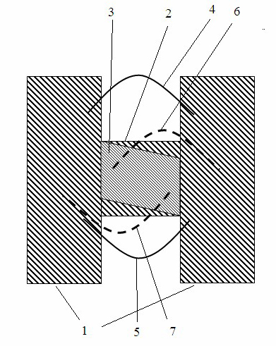
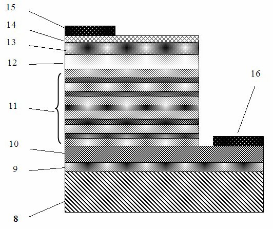
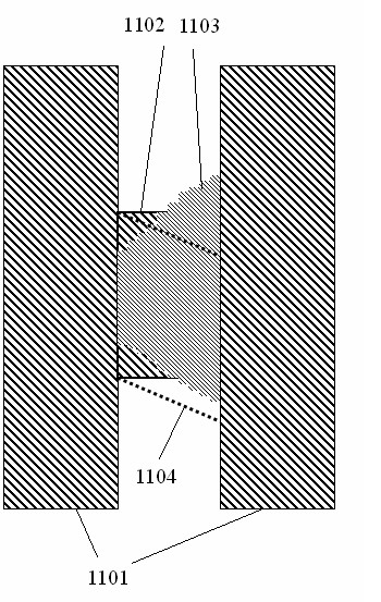
[0015] A gallium nitride semiconductor light-emitting diode with a tilted quantum well structure aims to neutralize the adverse effects of polarization effects through the optimization and design of the indium composition in the quantum well, so that the spatially separated electrons and holes The wave function increases the overlap, thereby improving the efficiency of radiative recombination, thereby improving the light efficiency of the LED. One embodiment of the metal organic compound deposition growth epitaxial layer of the present invention will be described below.

[0016] 1) A low-temperature gallium nitride layer 9 with a thickness of about 500 nm is grown on the sapphire substrate 8, the growth temperature is controlled between 500-600 degrees Celsius, and the growth pressure is between 400-700 Torr.

[0017] 2) An N-type gallium nitride layer 10 with a thickness of 2500nm is grown on the low-temperature gallium nitride layer 9, the growth temperature is controlled at...


PUM


Abstract

The invention discloses a gallium nitride semiconductor light-emitting diode with a tilt quantum well structure. By means of an energy band engineering design, an InGaN quantum well is designed to be a tilt structure so as to modulate the forbidden band width of the well. According to the invention, a polarization electric field produced due to a polarization effect in the quantum well can be overcome so as to make the distribution of electrons and holes more uniform, and thus, the quantum efficiency of the light-emitting diode is increased.

Description

technical field [0001] The invention relates to the field of gallium nitride semiconductor epitaxial design and growth, specifically through the energy band engineering design and the optimization of the quantum well structure to promote the wave function overlap of electrons and holes in the well, thereby realizing the quantum efficiency of gallium nitride semiconductor light-emitting diodes and improvement of luminous efficiency. Background technique [0002] For GaN semiconductor light-emitting diodes grown on the C-plane of a sapphire substrate, due to the existence of the C-plane polarization effect, a polarization potential field exists in the quantum well, which makes the conduction band and valence band tilt in the well, and the electrons and space Holes are spatially separated. It will have two adverse effects: one is to redshift the emission wavelength of the quantum well, and the other is to reduce the efficiency of radiative recombination in the well. The forme...

Claims


Application Information

Patent Timeline
Patent Type & Authority Applications(China)
IPC IPC(8): H01L33/06H01L33/30
Inventor 李文兵王江波董彬忠杨春艳
Owner HC SEMITEK CORP
Why Eureka
Try Eureka