Preparation method for super-lens with plane-shaped imaging surface by using secondary ion beam etching technology

A technology of ion beam etching and imaging surface, which is applied in the process of producing decorative surface effects, lens, microstructure technology, etc., can solve the problem that the imaging surface is a curved surface, etc., achieve uniform deposition thickness, wide application range and prospects , the effect of reducing the precipitation of particles

Active Publication Date: 2012-08-15
INST OF OPTICS & ELECTRONICS - CHINESE ACAD OF SCI
View PDF5 Cites 5 Cited by
  • Summary
  • Abstract
  • Description
  • Claims
  • Application Information

AI Technical Summary

Problems solved by technology

[0005] The technical problem to be solved by the present invention is: aiming at the problem that the imaging surface of the existing super-lens used for reducing super-resolution imaging is a curved surface, a method for preparing a super-lens with a flat imaging surface by using two ion beam etching techniques is proposed

Method used


Image

  • Preparation method for super-lens with plane-shaped imaging surface by using secondary ion beam etching technology
  • Preparation method for super-lens with plane-shaped imaging surface by using secondary ion beam etching technology
  • Preparation method for super-lens with plane-shaped imaging surface by using secondary ion beam etching technology

Examples


Embodiment 1

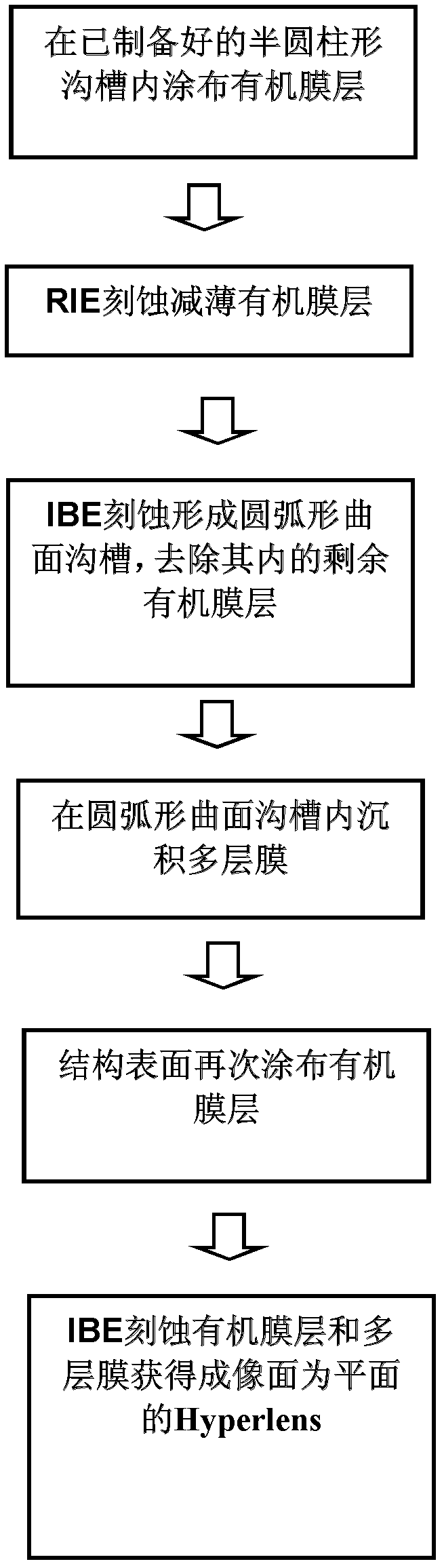
[0029] Embodiment 1, on the arc-shaped groove that diameter depth is 150nm, prepare the hyperlens that imaging surface is plane, and manufacturing process is as follows:

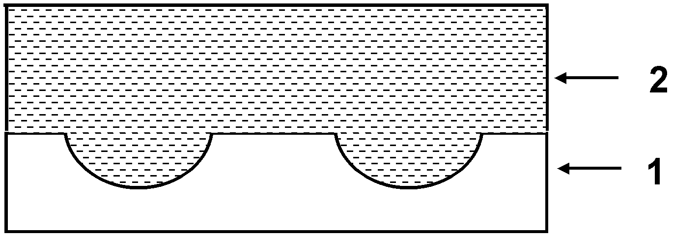
[0030] (1) On a semi-cylindrical trench prepared on a 1mm thick quartz substrate, AR-P3100 photoresist was coated by spin coating. In order to fill up the semi-cylindrical grooves, a method of coating multiple times at a spin coating speed of 2000rpm / 15sec was used. After multiple coatings, when the coating thickness of AR-P3100 reaches 4.6 microns, the semi-cylindrical grooves are filled, as figure 2 As shown, 1 represents the substrate material quartz; 2 represents various types of photoresist.

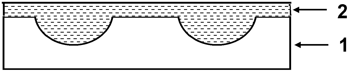
[0031] (2) Thinning the AR-P3100 photoresist by RIE etching, the etching power is 100W, the etching gas is oxygen, the flow rate is 50sccm, and the etching time is 10 minutes and 30 seconds, such as image 3 As shown, 1 represents the substrate material quartz; 2 represents various types of photoresist.

[003...

Embodiment 2

[0036] Embodiment 2, on the circular arc-shaped groove that diameter depth is 200nm, prepare the hyperlens that imaging plane is plane, and manufacturing process is as follows:

[0037] (1) On a semi-cylindrical trench prepared on a 1mm thick quartz substrate, AR-P3100 photoresist was coated by spin coating. In order to fill up the semi-cylindrical grooves, a method of coating multiple times at a spin coating speed of 2000rpm / 15sec was used. After multiple coatings, when the coating thickness of AR-P3100 reaches 4.8 microns, the semi-cylindrical grooves are filled, as figure 2 As shown, 1 represents the substrate material quartz; 2 represents various types of photoresist.

[0038] (2) Thinning the AR-P3100 photoresist by RIE etching, the etching power is 100W, the etching gas is oxygen, the flow rate is 50sccm, and the etching time is 11 minutes and 30 seconds, such as image 3 As shown, 1 represents the substrate material quartz; 2 represents various types of photoresist. ...


PUM

PropertyMeasurementUnit
thicknessaaaaaaaaaa
thicknessaaaaaaaaaa
etching poweraaaaaaaaaa

Abstract

The invention provides a preparation method for a super-lens with a plane-shaped imaging surface by using a secondary ion beam etching technology. The preparation method mainly comprises the following steps of: etching a semi-cylindrical groove by utilizing IBE (Ion Beam Etching) to obtain a circular-arc-shaped curve groove which has the same curvature radius as the semi-cylindrical groove and has a reduced diameter depth; then depositing a plurality of films in the circular-arc-shaped curve groove; and then, etching the plurality of films by utilizing the IBE to obtain the super-lens with the plane-shaped imaging surface. The preparation method can manufacture the plane-shaped super-lens without preparing a thin film with non-uniform thickness, and can obtain the circular-arc-shaped curve groove which has the same curvature as the semi-cylindrical groove and has the random diameter depth; the plurality of films with uniform thickness are deposited on the circular-arc-shaped curve groove and then the super-lens with the plane-shaped imaging surface is prepared on the circular-arc-shaped curve groove through the IBE etching technology. The preparation method only needs to adopt the conventional ion beam etching technology, a thin film depositing technology and a reaction ion etching technology to obtain the circular-arc-shaped curve groove which has the same curvature as the semi-cylindrical groove and has the random diameter depth, and the super-lens with the plane-shaped imaging surface can be prepared on the base.

Description

technical field [0001] The invention relates to the technical field of super-lens preparation, in particular to a method for preparing a super-lens whose imaging surface is a plane by using two ion beam etching techniques. Background technique [0002] It is well known that conventional lithographic resolution is limited by the diffraction limit. For this reason, research on super-resolution lithographic imaging that breaks through the diffraction limit is particularly important. Metalenses deposit periodic metal and dielectric film layers in semi-cylindrical grooves to form an artificial material suitable for evanescent wave transmission, thereby achieving reduced or enlarged super-resolution lithographic imaging. The application of metalens used to realize zoom-out super-resolution imaging is greatly limited because the imaging surface is a curved surface, so the preparation of a metalens with a flat imaging surface can be used for nanolithography imaging, sensing, plasma...

Claims


Application Information

Patent Timeline
Patent Type & Authority Applications(China)
IPC IPC(8): B81C1/00G02B3/00
Inventor 罗先刚赵泽宇王长涛王彦钦高平刘玲冯沁黄成杨磊磊陶兴
Owner INST OF OPTICS & ELECTRONICS - CHINESE ACAD OF SCI
Why Eureka
Try Eureka