Array substrate, manufacturing method thereof and display device

A technology for an array substrate and a manufacturing method, which is applied in the fields of an array substrate and its manufacturing method, and a display device, and can solve problems such as reducing thin film transistors, changes in material characteristics, and increasing equipment investment, so as to improve stability, reduce the number of times, and reduce costs Effect

Inactive Publication Date: 2012-08-22
BOE TECH GRP CO LTD
View PDF3 Cites 20 Cited by
  • Summary
  • Abstract
  • Description
  • Claims
  • Application Information

AI Technical Summary

Problems solved by technology

[0002] Indium gallium zinc oxide (IGZO) is a research hotspot of oxide semiconductor materials at the present stage. Its carrier mobility can reach 10, which is more than 10 times that of amorphous silicon. For large-area and ultra-fine panels , which can improve the response speed very well and reduce the size of thin film transistors (Thin Film Transistor, TFT). It is widely used, but because its material is easily affected by external conditions such as water vapor, oxygen, etc., the material properties will change
[0003] For general backplanes (i.e. array substrates), mass production at this stage is mainly LTPS (low temperature polysilicon), which has been mass-produced by Samsung, but due to the ELA process, it requires a lot of modification of existing equipment and increased investment in equipment

Method used


Image

  • Array substrate, manufacturing method thereof and display device
  • Array substrate, manufacturing method thereof and display device
  • Array substrate, manufacturing method thereof and display device

Examples


Embodiment 1

[0063] The specific description of the fabrication process of the array substrate in this embodiment is as follows:

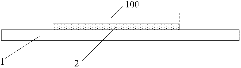
[0064] First, an oxide semiconductor layer pattern 2 is formed on a glass substrate 1 . Such as figure 1 As shown, it is a cross-sectional view of an oxide semiconductor layer pattern 2 formed on a glass substrate. The formation process is: depositing an oxide semiconductor thin film on a glass substrate 1. The material of the oxide semiconductor is IGZO or ZnO, and its thickness is between Coating photoresist on the oxide semiconductor film, using a mask to expose and develop the photoresist, retaining the photoresist in the pattern area 100 of the semiconductor layer; etching away the exposed oxide semiconductor film, and removing the remaining photoresist to form the oxide semiconductor layer pattern 2.

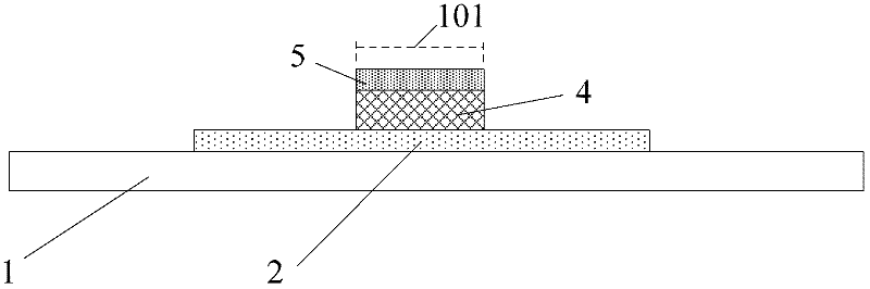
[0065] Next, a gate insulating layer pattern 4 and a gate pattern 5 are formed on the oxide semiconductor layer pattern 2 . Such as figure 2 As shown...

Embodiment 2

[0073] Another manufacturing method of the above-mentioned array substrate in this embodiment is as follows:

[0074] Such as Figure 9 As shown, an oxide semiconductor film, an insulating film and a gate metal film are sequentially deposited on a glass substrate 1 . The material of the oxide semiconductor thin film is IGZO or ZnO, and its thickness is between The material of the insulating film can be silicon nitride, silicon oxide, or aluminum oxide, etc. The material of the gate metal can be metals such as aluminum, copper, or alloys of metals such as aluminum and neodymium. The thickness of the insulating film is

[0075] Such as Figure 10 As shown, the photoresist 12 is coated on the gate metal film, and the photoresist 12 is exposed and developed through a double-tone mask (half-tone mask or gray-tone mask), and the pattern area of ​​the metal diffusion layer is reserved. 104, the photoresist 12 of the gate insulating layer, the gate and the gate line pattern area...

Embodiment 3

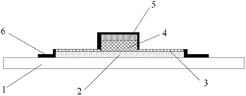
[0085] This embodiment provides an array substrate, which can be prepared by the method of the above-mentioned embodiment 1 or embodiment 2, and its structure is as follows Figure 8 As shown, it includes: a semiconductor layer 2 formed on a glass substrate 1 , a gate insulating layer 4 , a gate 5 , a barrier layer 6 , a passivation layer 7 , source and drain electrodes 8 and a pixel electrode 9 . A gate insulating layer 4 and a gate 5 are sequentially formed on the semiconductor layer 2 . The gate insulating layer 4 and the gate 5 are located in the middle of the semiconductor layer 2 and have the same shape and size. A metal diffusion layer 2 is also formed on the region of the semiconductor layer 2 not covered by the gate insulating layer 4 . Its formation process is as described in embodiment 1 or embodiment 2, deposits a layer of metal film on semiconductor layer 2, is preferably Al (because the diffusivity of Al is better, and can form dense protective layer after oxida...


PUM


Abstract

The invention discloses a manufacturing method of an array substrate, which relates to the technical field of display and comprises the following steps of: S1, forming graphs of a semiconductor layer, a gate insulation layer, a grid electrode and a grid line on the substrate; S2, forming a metal diffusion layer on the semiconductor graph which is not covered by the gate insulation layer on the substrate after step 1, and forming barrier layers in other areas; S3, forming a passivation layer on the substrate after step 2; and S4, forming graphs of a through hole, a source drain, a data line and a pixel electrode on the passivation layer, wherein the source drain is connected with the metal diffusion layer through the through hole. The invention also discloses an array substrate and a display device. Compared with the conventional mask manufacturing process more than four times, the process flow of the manufacturing method disclosed by the invention is reduced, and the process cost is reduced.

Description

technical field [0001] The present invention relates to the field of display technology, in particular to an array substrate, a manufacturing method thereof, and a display device. Background technique [0002] Indium gallium zinc oxide (IGZO) is a research hotspot of oxide semiconductor materials at the present stage. Its carrier mobility can reach 10, which is more than 10 times that of amorphous silicon. For large-area and ultra-fine panels , which can improve the response speed very well and reduce the size of thin film transistors (Thin Film Transistor, TFT). It is widely used, but because its material is easily affected by external conditions such as water vapor, oxygen, etc., the material properties will change. [0003] For general backplanes (array substrates), LTPS (Low Temperature Polysilicon) is currently mass-produced at Samsung, but it requires a lot of modification of existing equipment and increased equipment investment due to the ELA process. OLED backplane...

Claims


Application Information

Patent Timeline
Patent Type & Authority Applications(China)
IPC IPC(8): H01L21/77H01L27/12
CPCH01L27/1225H01L29/66969H01L29/7869H01L21/02304H01L29/78618H01L21/02365H01L21/76841H01L21/8234H01L27/1288H01L29/66742H01L27/127H01L29/22H01L29/24H01L29/78606H01L29/78696
Inventor 戴天明姚琪张锋曹占锋
Owner BOE TECH GRP CO LTD
Why Eureka
Try Eureka