
Vibration transducer
A technology of vibrating transducer and vibrating beam, which is applied in the direction of fluid, instrument, and electromagnetic means using vibration, can solve the problems of ineffective electrostatic force and narrowing of distance, prevent mode crossing and reduce contact. area, the effect of improving vibration stability
Patent Information
- Authority / Receiving Office
- CN · China
- Patent Type
- Applications(China)
- Current Assignee / Owner
- Publication Date
- 2012-09-19
Smart Images
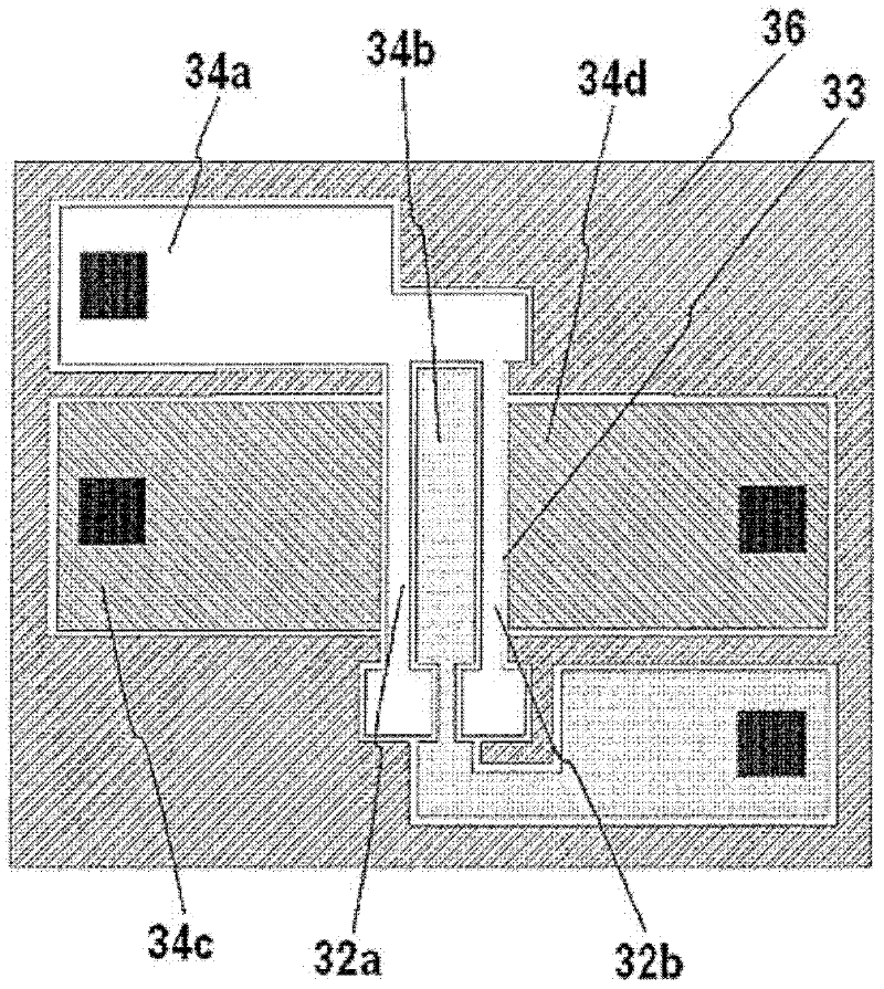
Figure 1 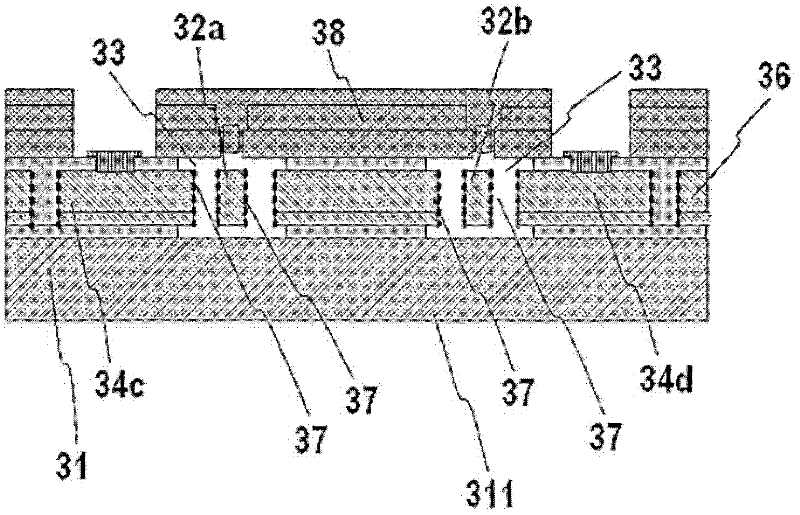
Figure 2 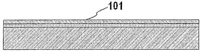
Figure 3
Abstract
Description
technical field
[0001] The invention relates to a vibration transducer. Background technique
[0002] Figure 29 to Figure 38 is a diagram for explaining the structure of a main part as an example of the prior art generally adopted so far.
[0003] Figure 29 is a diagram for explaining the assembly structure of the main part. Figure 30 to Figure 38 is a diagram for explaining the process of making it.
[0004] Description will be made in terms of manufacturing processes.
[0005] exist Figure 30 In the present invention, a silicon oxide film 10a is formed and patterned on an N-type silicon single crystal substrate 1 .
[0006] The portion from which the oxide film has been removed is undercut to form a concave portion, and doping with a concentration of 10 18 cm -3 Selective epitaxial growth of p-type silicon with boron to grow p+ monocrystalline silicon layer 11 .
[0007] Next, by doping with a concentration of at least 3×10 19 cm -3 The p-type silicon of boro...
Examples
Embodiment Construction
[0145] Hereinafter, the present invention will be described in detail with reference to the accompanying drawings.
[0146] Figure 1A-1B as well as Figure 2-Figure 15 is a diagram for explaining the structure of the main part of the embodiment of the present invention.
[0147] Figure 1A-1B is a diagram for explaining the assembly structure of the main part. Figure 1A is the floor plan of the main part, Figure 1B is its cross-sectional view. Figure 1 to Figure 15 is a diagram for explaining the manufacturing process.
[0148] In the attached figure, represented by the Figure 29 Components marked with the same reference numerals have the same function accordingly.
[0149] The following only describes the Figure 29 different parts.
[0150] exist Figure 1A and Figure 1B , each of the first and second vibrating beams 32 a and 32 b is arranged in a vacuum chamber 33 . Tensile strain is applied to the substrate 31 in these vibration beams. The first and sec...