A method of fabricating a multilayer organic liquid crystal polymer substrate structure

A liquid crystal polymer and substrate technology, applied in semiconductor/solid-state device manufacturing, instruments, electrical components, etc., can solve the problems of poor reworkability of source chips, rupture of embedded active chips, low production efficiency, etc. Good reworkability, excellent high frequency performance, and the effect of avoiding pressure damage problems

Active Publication Date: 2016-01-20
NAT CENT FOR ADVANCED PACKAGING CO LTD
View PDF4 Cites 34 Cited by
  • Summary
  • Abstract
  • Description
  • Claims
  • Application Information

AI Technical Summary

Problems solved by technology

[0010] In addition, US Patent No. 2010 / 0201003A1 relates to a method of embedding radio frequency micro-electromechanical switches into a double-layer liquid crystal polymer substrate, such as figure 1 As shown, the entire packaging structure 10 mainly includes a first layer of liquid crystal polymer 12, an electronic component 14 and a second layer of liquid crystal polymer 16, where the first layer of liquid crystal polymer 12 is used to support the electronic component 14, and the electronic component 14 A radio-frequency micro-electromechanical switch is used, and the first layer of liquid crystal polymer 12 and the second liquid crystal polymer 16 are connected by a low-melting liquid crystal polymer 18 to realize a radio-frequency micro-electromechanical switch in a double-layer liquid crystal polymer film. The sealed embedded structure, but if this structure is used to embed other components, it needs to be stacked up layer by layer, which is time-consuming and labor-intensive, and will inevitably bring low production efficiency and high cost, especially "stacking" The process of connecting embedded chips is easy to cause the rupture of embedded active chips, and the reworkability of active chips is not good, so a higher level of good chips must be required

Method used


Image

  • A method of fabricating a multilayer organic liquid crystal polymer substrate structure
  • A method of fabricating a multilayer organic liquid crystal polymer substrate structure
  • A method of fabricating a multilayer organic liquid crystal polymer substrate structure

Examples


Embodiment Construction

[0056] In order to make the object, technical solution and advantages of the present invention clearer, the present invention will be described in further detail below in conjunction with specific embodiments and with reference to the accompanying drawings.

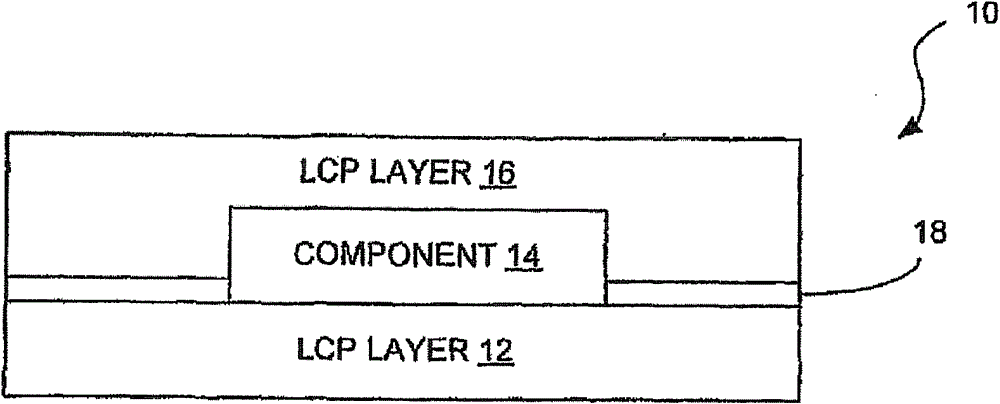
[0057] The invention is based on a new type of packaging material - liquid crystal polymer, which not only embeds active and passive devices into the multi-layer organic substrate at the same time, but also adopts a one-time pressing process to form a multi-layer liquid crystal polymer substrate. Implement the concept of system-in-package. Different from the high sintering temperature of low-temperature co-fired ceramics, the lamination temperature of the multilayer organic substrate is not very high. Not only can passive devices be embedded in the multilayer substrate, but also active devices can be embedded in the substrate. Moreover, it will not damage active devices, and is compatible with traditional semiconductor pr...


PUM

PropertyMeasurementUnit
melting pointaaaaaaaaaa
thicknessaaaaaaaaaa
melting pointaaaaaaaaaa

Abstract

The invention discloses a method for making a multi-layer organic liquid crystal polymer (LCP) substrate structure. The method comprises the following steps: providing a first LCP core substrate and a second LCP core substrate; connecting an active device to the first LCP core substrate in an inverted manner; arranging a passive device on the second LCP core substrate by means of surface mounting, sequentially overlapping and stacking the second LCP core substrate mounted with the passive device, an LCP dielectric layer and the first LCP core substrate connected with the active device in an inverted manner, and thermoforming to obtain the multi-layer LCP substrate structure embedded with both the active device and the passive device. The multi-layer LCP substrate structure can be used for making a microwave / millimeter wave system level module and has the characteristic of achieving a system with high density, small size, high performance, high frequency, low value and low consumption.

Description

technical field [0001] The present invention relates to the technical field of organic liquid crystal polymer (Liquid Crystal Polymer, LCP) substrate manufacturing, in particular, to a method for manufacturing a multi-layer organic liquid crystal polymer substrate structure, the multi-layer organic liquid crystal polymer substrate structure is embedded with active Devices and passive devices, using two kinds of liquid crystal polymer films with different melting points, so as to realize high-frequency system-in-package with high density and three-dimensional structure. Background technique [0002] At present, there is an urgent need at home and abroad to develop substrate materials that can adapt to high-speed signal transmission, high-density wiring and high-frequency circuits. This substrate can simultaneously integrate RF active and passive devices in the same material, while achieving small, high-density , high-performance and low-power low-value high-frequency modules....

Claims


Application Information

Patent Timeline
Patent Type & Authority Patents(China)
IPC IPC(8): H01L21/50H01L21/56H05K3/30G02F1/1333
Inventor 张霞曹立强
Owner NAT CENT FOR ADVANCED PACKAGING CO LTD
Why Eureka
Try Eureka