Method for manufacturing active area of indium arsenide/indium phosphide quantum dot laser

An indium arsenide and laser technology, applied in lasers, phonon exciters, laser parts, etc., can solve the problems of reducing the optical performance of quantum dot lasers, reducing the luminous efficiency of quantum dots, and increasing quantum dots.

Active Publication Date: 2012-09-19
JIANGSU HUAXING LASER TECH CO LTD
View PDF5 Cites 6 Cited by
  • Summary
  • Abstract
  • Description
  • Claims
  • Application Information

AI Technical Summary

Problems solved by technology

The wavelength adjustment technology reported in the literature is mainly to adjust the wavelength by inserting a GaAs thin layer under the quantum dot or doping Ga components into the quantum dot, but the result is t

Method used


Image

  • Method for manufacturing active area of indium arsenide/indium phosphide quantum dot laser
  • Method for manufacturing active area of indium arsenide/indium phosphide quantum dot laser
  • Method for manufacturing active area of indium arsenide/indium phosphide quantum dot laser

Examples


Embodiment Construction

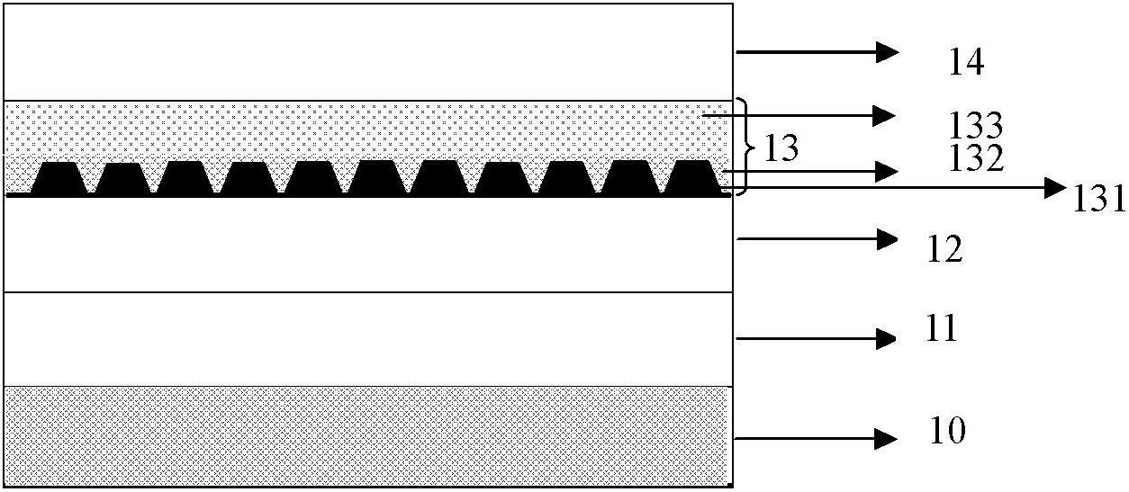
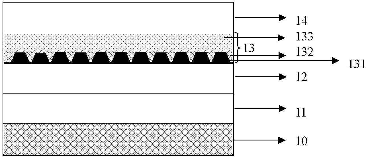
[0016] See figure 1 As shown, the present invention provides a method for manufacturing the active region of an indium arsenide / indium phosphide quantum dot laser, which includes the following steps:

[0017] Step 1: Select an indium phosphide substrate 10, the substrate is an n+ type InP single wafer, the crystal orientation is (100), the thickness is 325-375um, and the doping concentration is (1-3)×10 18 cm -3 .

[0018] Step 2: Epitaxially grow a layer of indium phosphide buffer layer 11 on the indium phosphide substrate 10, the growth temperature of the indium phosphide buffer layer 11 is 645°C, the thickness is 300 nm, and the molar ratio of the V group to the III group source is 200.

[0019] Step 3: Deposit a lattice-matched InGaAsP thin layer 12 on the indium phosphide buffer layer 11. The growth temperature of the InGaAsP thin layer 12 is 645°C; the deposition thickness is 100nm; the growth rate is 0.5nm / s, the molar flow rate (V / III) of the group V source As and P and the...


PUM

PropertyMeasurementUnit
Deposition thicknessaaaaaaaaaa
Thicknessaaaaaaaaaa
Growth temperatureaaaaaaaaaa

Abstract

The invention provides a method for manufacturing an active area of an indium arsenide/indium phosphide quantum dot laser. The method comprises the following steps of: step 1, selecting an indium phosphide substrate; step 2, epitaxially growing an indium phosphide buffering layer on the indium phosphide substrate; step 3, depositing a lattice matched indium-gallium-arsenic-phosphorus thin layer on the indium phosphide buffering layer; step 4, epitaxially growing a multi-periodical indium arsenide quantum dot active layer; and step 5, depositing an indium-gallium-arsenic-phosphorus cover layeron the indium arsenide quantum dot active layer. According to the method provided by the invention, the purposes of keeping good optical properties and tuning the light-emitting wavelength are achieved by changing a five-group protection source flow to restrain an As/P exchange effect, controlling the appearance of a quantum dot and combining a two-step cover layer growth process in a growth pause interval of an indium arsenide/indium phosphide quantum dot. The method provided by the invention can be used for controllably adjusting the InAs/InP quantum dot light-emitting wave in a range of 1.3-1.7 microns (num) to 400 nm.

Description

Technical field [0001] The invention belongs to the field of semiconductor technology, and particularly refers to a method for manufacturing the active region of an indium arsenide / indium phosphide quantum dot laser. The method is based on a quantum device of low-dimensional semiconductor nanostructure quantum dot material, such as arsenide (gallium) An epitaxial growth method for the active region of indium / indium phosphide (In(Ga)As / InP) quantum dot lasers. Specifically, it relates to adjusting the emission wavelength of the indium arsenide / indium phosphide quantum dot material by controlling the group V protection source during the growth pause. Background technique [0002] The new generation of high-speed optical communication systems urgently needs low-power, high-performance, long-wavelength semiconductor laser light sources. As an important candidate for transmitting signal carrier light waves or light sources, semiconductor quantum dot lasers have received great attenti...

Claims


Application Information

Patent Timeline
IPC IPC(8): H01S5/343
Inventor 罗帅季海铭杨涛
Owner JIANGSU HUAXING LASER TECH CO LTD
Why Eureka
Try Eureka