

Method for manufacturing micro-nano pyramid gallium nitride based light-emitting diode array with vertical structure
A technology of micro-nano pyramids and light-emitting diodes, which is applied to electrical components, circuits, semiconductor devices, etc., and can solve the problems of large reverse leakage and low yield
- Summary
- Abstract
- Description
- Claims
- Application Information
AI Technical Summary
Problems solved by technology
Method used
Image

Examples
Embodiment
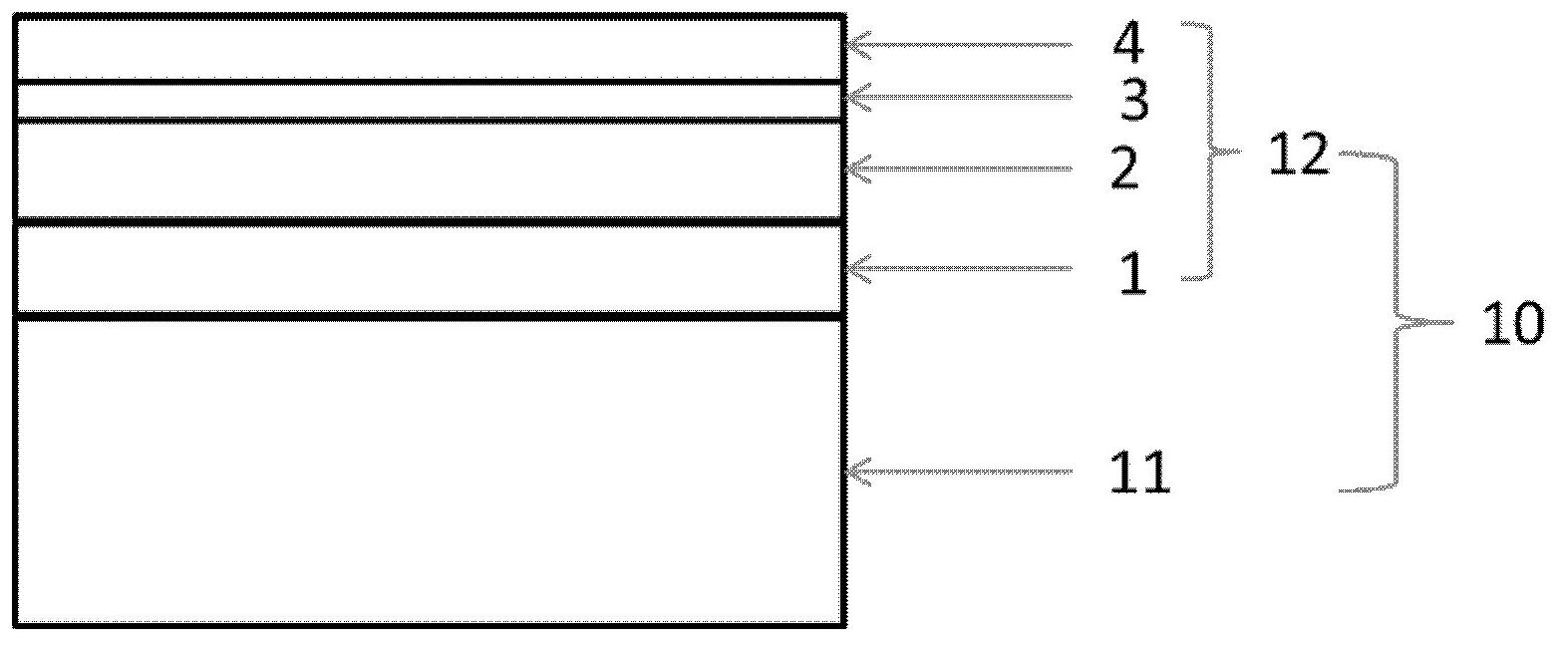
[0036] see Figure 1 to Figure 5 As shown, the present invention provides a method for making a micro-nano pyramid gallium nitride-based vertical structure light-emitting diode array, comprising the following steps:
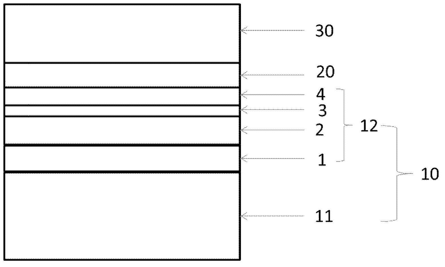
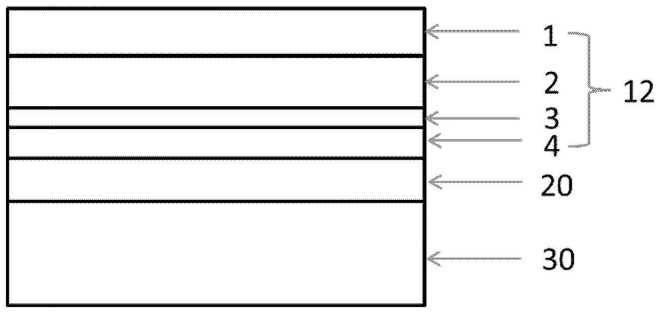
[0037] Step 1: Select an epitaxial structure 10 including a sapphire substrate 11 and a gallium nitride LED layer 12 in sequence. The gallium nitride LED layer 12 includes an unintentionally doped gallium nitride layer 1 (2 μm), an n-type gallium nitride layer 2 (2 μm), a quantum well layer 3 (100 nm), and a p-type gallium nitride layer 4 (100 nm);
[0038] Step 2: Depositing a metal layer 20 on the p-type gallium nitride layer 4, the metal layer 20 is Ni\Ag\Pt\Au multilayer metal;
[0039] Step 3: Electroplating Cu\Ni multilayer metals sequentially on the metal layer 20 by an electroplating method to form a substrate
[0040] Step 4: using a laser lift-off method to separate the sapphire substrate 11 from the epitaxial layer 12;
[0041] Step 5: Etching the s...
PUM
 Abstract
Description
Claims
Application Information