
Wet etching method for ZnO-based transparent conductive film

A transparent conductive thin film, wet etching technology, used in circuits, electrical components, semiconductor devices, etc., can solve the problems of fast etching rate and difficult control, achieve low etching cost, inhibit lateral etching, select wide range of effects

Active Publication Date: 2012-10-03
SUN YAT SEN UNIV
View PDF8 Cites 6 Cited by
  • Summary
  • Abstract
  • Description
  • Claims
  • Application Information

AI Technical Summary

Problems solved by technology

[0004] The purpose of the present invention is to overcome the problems that the etching rate is too fast, difficult to control, and serious side etching in the current strong acid etching process, and provide a controllable, high-precision wet etching of ZnO-based transparent conductive film method

Method used


Image

  • Wet etching method for ZnO-based transparent conductive film
  • Wet etching method for ZnO-based transparent conductive film
  • Wet etching method for ZnO-based transparent conductive film

Examples


Embodiment 1

[0021] The Ga-doped ZnO-based transparent conductive film grown by the MOCVD method is glued and glued. use figure 1 The photoresist shown in the photoetching plate performs photolithography and development on the Ga-doped ZnO transparent conductive film, removes unnecessary photoresist, and obtains pattern structures with different line widths.

[0022] Mix glacial acetic acid and water at a ratio of 1:1, etch the above-mentioned Ga-doped ZnO-based transparent conductive film for 4 minutes, etch away the ZnO exposed from the glue, and then remove the glue.

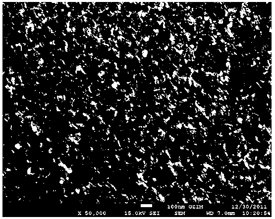
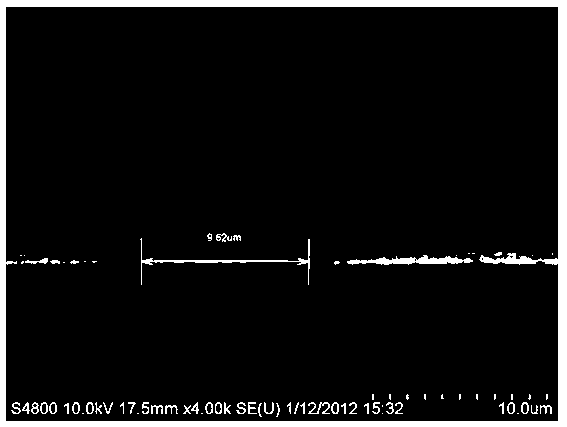
[0023] Scanning electron microscope (SEM) image of Ga-doped ZnO transparent conductive film grown by MOCVD before etching figure 2 Shown; the partial side scanning electron microscope (SEM) image formed by etching the ZnO-based thin film with acetic acid solution is shown in image 3 Shown; The scanning electron microscope (SEM) image of the partial cross-section formed by etching the ZnO-based film with acetic acid s...

Embodiment 2

[0025] The Al-doped ZnO-based transparent conductive film grown by MOCVD method has a film thickness of about 250nm, which is coated with glue and shaken off. use figure 1 The photoresist plate shown in the photolithography and development of the Al-doped ZnO transparent conductive film removes the unnecessary photoresist to obtain the pattern of the desired structure.

[0026] Mix glacial acetic acid and water at a ratio of 1:1 to etch the above-mentioned Al-doped ZnO-based transparent conductive film for 5 minutes to etch the ZnO-TCL exposed from the glue.

Embodiment 3

[0028] The Ga-doped ZnO-based transparent conductive film grown by MOCVD method has a film thickness of about 250nm, which is coated with glue and shaken off. use figure 1 The photoresist shown in the photoetching plate performs photolithography and development on the Ga-doped ZnO-based transparent conductive film, removes unnecessary photoresist, and obtains the desired etched structure pattern. The above-mentioned Ga-doped ZnO transparent conductive film was etched with ammonium chloride with a mass concentration of 15%, and the ZnO-TCL exposed from the glue could be etched away for 40 minutes.


PUM


Abstract

The invention discloses a wet etching method for a ZnO-based transparent conductive film The wet etching method comprises the following steps: coating photoresist on a substrate deposited with the ZnO-based transparent conductive film; carrying out exposure and development and removing part of the photoresist so that the substrate to be etched is exposed; baking the substrate; proportioning with weak acids and deionized water to form a weak acid solution; putting the substrate to be etched into the weak acid solution for etching for 1-10000 seconds; washing with deionized water; removing the photoresist with an organic solution; and measuring the etching depth and the profile of the etched pattern. A weak acid solution wet etching process is adopted in the method, and the method has the advantages of simple operation, low cost, controllable etching rate, high etching precision and the like, and can be applied to a pattern processing technology of ZnO-based transparent electrodes in the fields of solar batteries, panel display, LEDs (light-emitting diodes) and the like, so that the industrial applications of the ZnO-based transparent conductive films the above fields are promoted.

Description

[0001] technical field [0002] The invention relates to a wet etching method for a ZnO-based transparent conductive film. Background technique [0003] Transparent conductive films are widely used in solar cells, semiconductor lighting, flat panel displays and other fields. At present, the transparent conductive film widely used in the industry is the first generation of transparent conductive film represented by Ni / Au, which has good electrical conductivity and material stability, but its major deficiency is that the maximum visible light transmittance is less than 75%. The second is the second-generation transparent conductive film represented by indium tin oxide (ITO), which has good electrical conductivity, but due to the large amount of precious metal In material used in it, its manufacturing cost is greatly increased, and it faces the problem of depletion of rare metal indium. Danger. ITO materials also have problems such as poor reliability, toxicity, environmental...

Claims


Application Information

Patent Timeline
Patent Type & Authority Applications(China)
IPC IPC(8): H01L21/02H01L33/42H01L31/0224
Inventor 裴艳丽吴锦壁江灏范冰丰王钢
Owner SUN YAT SEN UNIV
Learn More