AlGaInP light-emitting diode (LED) chip and cutting method for same

A technology of LED chips and cutting methods, applied in electrical components, circuits, semiconductor devices, etc., can solve the problems of high machine cost and labor cost, fast cutting knife wear, low product qualification rate, etc., to reduce labor and machine costs. cost, improve the brightness of the light, and increase the effect of the light-emitting area

Inactive Publication Date: 2012-10-03
东莞洲磊电子有限公司
View PDF7 Cites 14 Cited by
  • Summary
  • Abstract
  • Description
  • Claims
  • Application Information

AI Technical Summary

Problems solved by technology

[0003] The cutting method in the quaternary LED chip manufacturing process is the process of dividing the whole chip into a single crystal grain. In the prior art, the quaternary LED chip is cut in half and then completely cut with a diamond cutter. The cutting speed is low, the cutting knife wears fast, the life is short, the diamond cutting knife is expensive, and the demand for personnel and machines is relatively large, resulting in high machine costs and labor costs, and the cutting knife is in direct contact with the chip during cutting. Edges are prone to edge chipping, chipping and cracks, and the product qualification rate is low
[0004] The width of the traditional dicing knife is 20 μm to 25 μm, so after cutting, the cutting surface of the chip has a loss of about 25 μm to 30 μm, and the loss of the section is relatively large, resulting in great waste

Method used


Image

  • AlGaInP light-emitting diode (LED) chip and cutting method for same
  • AlGaInP light-emitting diode (LED) chip and cutting method for same

Examples


Embodiment 1

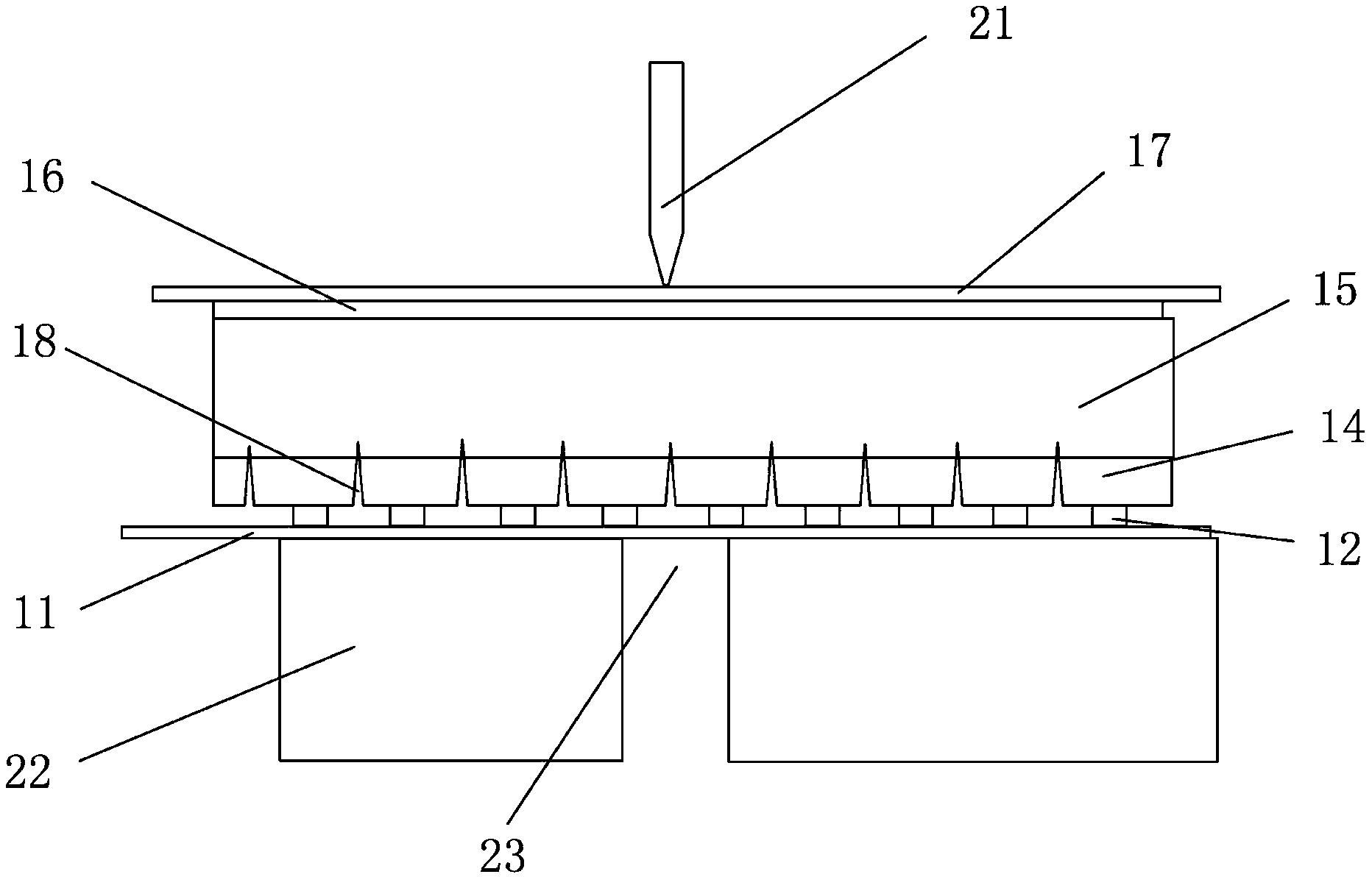
[0029] A kind of quaternary system LED chip of the present invention, as figure 1 as shown,

[0030] A GaAs substrate 15 is included as an epitaxial layer substrate. As a substrate material for quaternary red-yellow LED chips, GaAs has obvious advantages. GaAs has very stable chemical properties, good lattice matching with quaternary materials, and good electrical and thermal conductivity.

[0031] One side of the GaAs substrate 15 is epitaxially formed with an epitaxial layer 14 , that is, the PN junction of the LED chip.

[0032] The other side of the GaAs substrate 15 is plated with an Au thin film layer, which serves as the negative terminal 16 of the LED chip. Before the Au thin film layer is plated, the wafer needs to be cleaned by a chemical solution.

[0033] On the epitaxial layer 14 are deposited BeAu thin film layers arranged at equal intervals, and on the BeAu thin film layer is also deposited an Au thin film layer as the positive terminal 12 of the LED chip. ...

Embodiment 2

[0037] A cutting method of a quaternary LED chip of the present invention, such as figure 1 As shown, the positive end 12 of the LED chip is half-cut with a diamond cutter to form a cutting line 18, and the positive end 12 of the LED chips arranged at equal intervals is separated, and then the negative end 16 of the LED chip is cut along the edge with a splitter. Road 18 cuts off the half-cut LED chip. Generally speaking, the basic thickness of the LED chip is 100 μm-300 μm, and the depth of the corresponding cutting line 18 should be 25 μm-250 μm. The half-cut depth can ensure that the epitaxial layer 14 is completely cut off. , the GaAs substrate 15 is cut with traces to ensure that the GaAs substrate 15 is easily split along the cutting line 18 without cracking during cutting.

[0038] Specifically include the following steps:

[0039] (1) half-cut the LED chip with a diamond cutting knife of a cutting machine, and the half-cut depth is 25 μm to 250 μm to form a cutting li...


PUM


Abstract

The invention discloses an AlGaInP light-emitting diode (LED) chip, which comprises a GaAs substrate serving as an epitaxial layer substrate. An epitaxial layer is arranged on one surface of the GaAs substrate, and serves as a PN junction of the LED chip. An Au thin film is plated on the other surface of the GaAs substrate, and serves as the cathode end of the LED chip. BeAu thin films arranged at equal intervals are deposited on the epitaxial layer, and an Au thin film is deposited on the BeAu thin films to form the anode ends of the LED chip. A cutting method for the AlGaInP LED chip specifically comprises the following steps of: (1) half-cutting the LED chip on one surfaces of the anode ends of the LED chip by using a diamond cutter to form cutting channels to separate the uniformly arranged anode ends of the LED chip, wherein the LED chip is 100 to 300 mu m thick; (2) coating a blue film at the anode ends of the LED chip, and coating a Mylar film at the cathode end of the LED chip; and (3) placing the LED chip on a cleaving table of a cleaver in a way that the anode end of the LED chip is downward and the cathode end of the LED chip is upward, and pressing and breaking the LED chip along the cutting channels by using a cleaving knife of the cleaver, so that the LED chip forms independent crystal grains.

Description

technical field [0001] The invention discloses a quaternary LED chip and a cutting method thereof, belonging to the technical field of LED chip manufacturing. Background technique [0002] Quaternary LED chips are widely valued by the semiconductor lighting industry due to their high luminous efficiency, wide color range, and long service life. They have been widely used in various fields such as large-screen displays, traffic lights, landscape lighting, and automotive status displays. [0003] The cutting method in the quaternary LED chip manufacturing process is the process of dividing the whole chip into a single crystal grain. In the prior art, the quaternary LED chip is cut in half and then completely cut with a diamond cutter. The cutting speed is low, the cutting knife wears fast, the life is short, the diamond cutting knife is expensive, and the demand for personnel and machines is relatively large, resulting in high machine costs and labor costs, and the cutting kni...

Claims


Application Information

Patent Timeline
Patent Type & Authority Applications(China)
IPC IPC(8): H01L33/00H01L21/78
Inventor 陈昆男许智源王湘军戴世攀周晓莉方飞
Owner 东莞洲磊电子有限公司
Why Eureka
Try Eureka