Flexible organic electroluminescence display (OELD) and manufacture method thereof

A production method and electroluminescence technology, which are applied in the direction of electric solid device, semiconductor/solid state device manufacturing, circuits, etc., can solve the problems of poor temperature resistance, high roughness, and short life of OLED of plastic films, and achieve strong conductivity and flexibility. good effect

Inactive Publication Date: 2012-10-03
TRULY SEMICON
View PDF4 Cites 8 Cited by
  • Summary
  • Abstract
  • Description
  • Claims
  • Application Information

AI Technical Summary

Problems solved by technology

However, the plastic film has poor temperature resistance, and many high-temperature environments in the OLED manufacturing process cannot be tolerated by the plastic film; and the plastic film has poor water resistance, resulting in a short OLED life. In order to improve the water resistance, it is necessary to evaporate and coat multi-layer resistance. Water materials, resulting in complicated process, not suitable for mass production
Although the stainless steel film has good flexibility, temperature and water resistance, its roughness is too high, and it will still have a high roughness after polishing. It is too high for OLED devices and is still not suitable.

Method used


Image

  • Flexible organic electroluminescence display (OELD) and manufacture method thereof
  • Flexible organic electroluminescence display (OELD) and manufacture method thereof
  • Flexible organic electroluminescence display (OELD) and manufacture method thereof

Examples


Embodiment 1

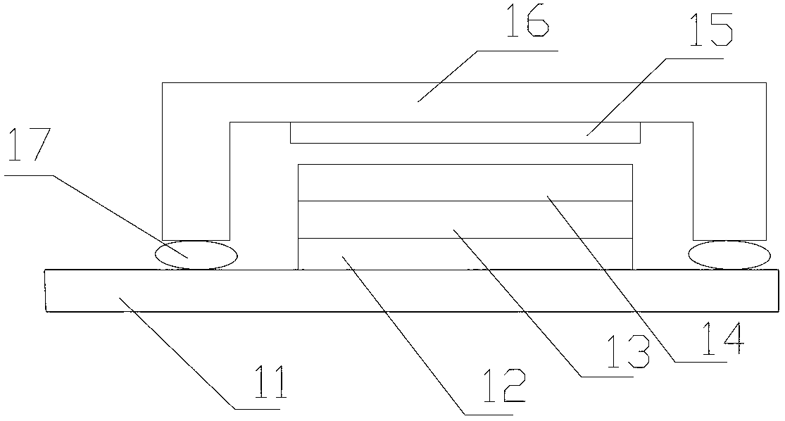
[0042] The method in this embodiment is used to fabricate a flexible OLED with a top emission structure, and the driving mode is passive, that is, PMOLED. The method of this embodiment specifically includes the following steps:

[0043] 1. Take an FPC base material, cut the FPC base material into an appropriate size, and clean it;

[0044] 2. Spin-coat photoresist on the second Cu layer 33, and perform exposure after pre-curing. The exposure pattern is designed according to the PMOLED electrode pattern; after development and main curing, put it into an acidic solution for acid etching, and the acid etching time depends on the thickness of the Cu layer and change; after stripping, the required first electrode pattern is obtained;

[0045] 3. Make an insulating protective layer and a cathode spacer post pattern on the first electrode pattern. This process is the same as the traditional PMOLED manufacturing process, so it will not be repeated here; through this step, a flexible ...

Embodiment 2

[0051] The method in this embodiment is used to fabricate a flexible OLED with a top emission structure, and the driving mode is active, that is, AMOLED.

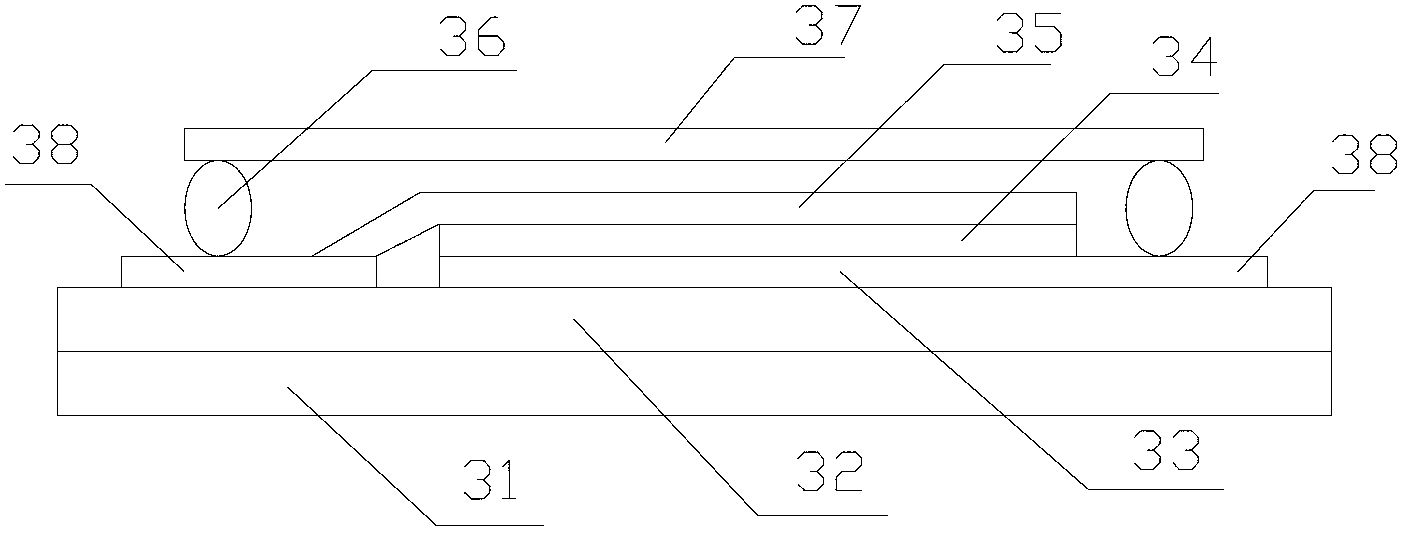
[0052] 1. Take an FPC substrate, cut it into an appropriate size, and clean it. FPC structure such as figure 2 , including a first Cu layer, a PI layer and a second Cu layer;

[0053] 2. Spin-coat photoresist on the second Cu layer, and perform exposure after pre-curing. The exposure pattern is designed according to the AMOLED first electrode pattern; after developing and main curing, put it into an acidic solution for acid etching. The acid etching time is obtained according to the Cu layer. The thickness varies; after stripping, the required first electrode pattern is obtained;

[0054] 3. Fabricate a TFT drive circuit on the first electrode pattern, the process is the same as the traditional AMOLED TFT substrate production process, and will not be repeated here; through this step, the TFT substrate is obtained;

[00...


PUM


Abstract

The invention discloses a manufacture method of a flexible organic electroluminescence display (OELD). The manufacture method comprises the following steps of: (1) taking an FPC (Flexible Printed Circuit) base material comprising a first Cu layer, a PI layer and a second Cu layer, and photoetching the second Cu layer to obtain a required first electrode pattern; (1) processing the first electrode pattern to obtain a substrate; (3) evaporating an organic electroluminescence material and a second electrode on the substrate in sequence; (4) packaging to form a device; and (5) binding IC (Integrated Circuit) to obtain the flexible OELD. According to the manufacture method of the flexible OELD, disclosed by the invention, FPC in COF (Chip on Flex) is used as the base material to manufacture the flexible OELD, is good in flexibility and strong in electroconductivity, and can be used to completely isolate the influence of water vapor to OELD, so that the advantages of a plastic thin film and a stainless sheet are combined, the permeation of the water vapor and oxygen on the surface of the base material can be isolated completely, and by adoption of a process of etching one Cu layer in the FPC, the manufacture method is suitable for mass production.

Description

technical field [0001] The invention relates to a manufacturing method of an organic electroluminescent display, in particular to a flexible organic electroluminescent display and a manufacturing method thereof. Background technique [0002] Organic electroluminescent display, or OLED for short, is a new type of flat panel display, because it has many advantages such as active light emission, high contrast, fast response speed, thin and light, etc., it is known as a new generation of display that can replace liquid crystal display (LCD for short) . The principle of luminescence is to insert various functional layers between the anode and the cathode, including charge injection layer, charge transport layer and light-emitting layer, and apply an appropriate voltage between the electrodes to make the device emit light. The structure diagram of OLED is shown in figure 1 As shown, it includes: substrate 11, generally made of glass ion; anode 12, generally ITO transparent condu...

Claims


Application Information

Patent Timeline
Patent Type & Authority Applications(China)
IPC IPC(8): H01L51/56H01L51/52H01L27/32
Inventor 苏君海张雪峰柯贤军何基强李建华
Owner TRULY SEMICON
Why Eureka
Try Eureka