Electromagnetic wave absorbing material with periodic structure, and preparation method thereof

An electromagnetic absorption and periodic structure technology, applied in chemical instruments and methods, electrical components, magnetic field/electric field shielding, etc., can solve the problems of limited absorption bandwidth, high volume density, narrow absorption bandwidth, etc., and improve the absorption bandwidth , low volume density, low cost effect

Inactive Publication Date: 2012-10-03
NAT UNIV OF DEFENSE TECH
View PDF3 Cites 25 Cited by
  • Summary
  • Abstract
  • Description
  • Claims
  • Application Information

AI Technical Summary

Problems solved by technology

However, the current magnetic absorbing materials are all using the traditional Dallenbach structure or multi-layer structure, which has a large volume density and a very limited absorbing bandwidth, which is difficult to meet the application requirements.
Therefore, it will be of great significance to design a new type of absorbing material that can effectively solve the problems of narrow absorption bandwidth and high density of existing magnetic absorbing materials.

Method used


Image

  • Electromagnetic wave absorbing material with periodic structure, and preparation method thereof
  • Electromagnetic wave absorbing material with periodic structure, and preparation method thereof
  • Electromagnetic wave absorbing material with periodic structure, and preparation method thereof

Examples


Embodiment 1

[0029] Kind of like Figure 4 ~ Figure 6 The electromagnetic absorbing material with a periodic structure shown in the present invention includes a magnetic absorbing material grid 2 and a dielectric block 1 made of dielectric material. The magnetic absorbing material grid 2 has a through hole and the dielectric block 1 It is embedded in the through holes of the magnetic absorbing material grid 2 according to a certain period. In this embodiment, the embedding according to a certain period specifically means that the embedding is arranged in a matrix to form a rectangular array of dielectric blocks.

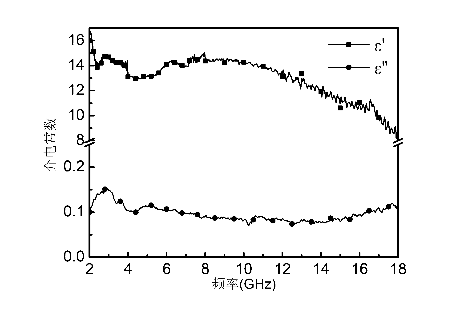
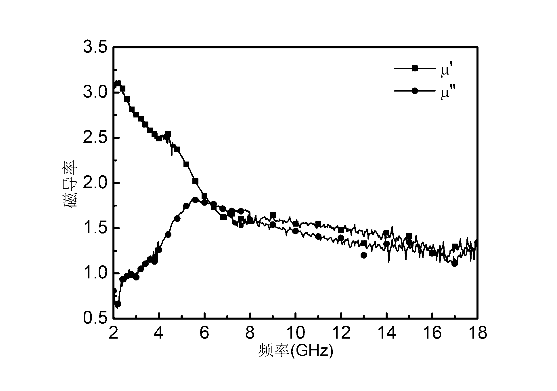
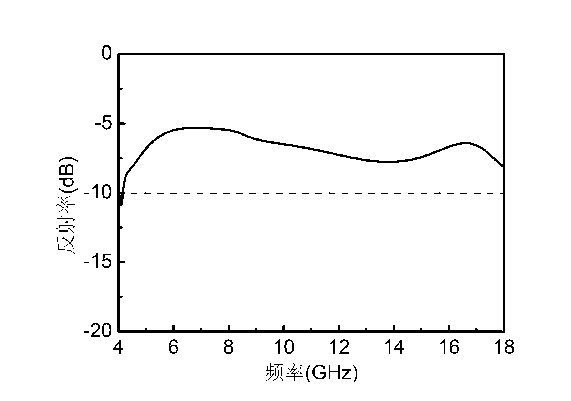
[0030] In this embodiment, the dielectric block 1 is cylindrical, with a bottom diameter of 10 mm, and the distance between the centers of two adjacent dielectric blocks 1 is 12.5 mm. The dielectric block 1 is made of epoxy resin material, and its relative dielectric constant is about 3, and the dielectric loss is negligible. The thickness of the entire electromagnetic absorbing ma...

Embodiment 2

[0037] Kind of like Figure 4 ~ Figure 5 The electromagnetic absorbing material with a periodic structure shown in the present invention includes a magnetic absorbing material grid 2 and a dielectric block 1 made of dielectric material. The magnetic absorbing material grid 2 has a through hole and the dielectric block 1 It is embedded in the through holes of the magnetic absorbing material grid 2 according to a certain period. In this embodiment, the embedding according to a certain period specifically means that the embedding is arranged in a matrix to form a rectangular array of dielectric blocks.

[0038] In this embodiment, the dielectric block 1 is cylindrical, with a bottom diameter of 8 mm, and the distance between the centers of two adjacent dielectric blocks 1 is 12.5 mm. The dielectric block 1 is made of epoxy resin material, and its relative dielectric constant is about 3, and the dielectric loss is negligible. The thickness of the entire electromagnetic absorbing mat...

Embodiment 3

[0042] Kind of like Figure 4 ~ Figure 5 The electromagnetic absorbing material with a periodic structure shown in the present invention includes a magnetic absorbing material grid 2 and a dielectric block 1 made of dielectric material. The magnetic absorbing material grid 2 has a through hole and the dielectric block 1 It is embedded in the through holes of the magnetic absorbing material grid 2 according to a certain period. In this embodiment, the embedding according to a certain period specifically means that the embedding is arranged in a matrix to form a rectangular array of dielectric blocks.

[0043] In this embodiment, the dielectric block 1 is cylindrical, with a bottom diameter of 11.5 mm, and the distance between the centers of two adjacent dielectric blocks 1 is 12.5 mm. The dielectric block 1 is made of epoxy resin material, and its relative dielectric constant is about 3, and the dielectric loss is negligible. The thickness of the entire electromagnetic absorbing ...


PUM

PropertyMeasurementUnit
diameteraaaaaaaaaa
diameteraaaaaaaaaa
thicknessaaaaaaaaaa

Abstract

The invention discloses an electromagnetic wave absorbing material with a periodic structure. The electromagnetic wave absorbing material comprises dielectric blocks formed by a magnetic wave absorbing material grid and a dielectric material, wherein the meshes on the magnetic wave absorbing material grid are through holes, and the dielectric blocks are embedded in the through holes of the magnetic wave absorbing material grid according to a certain periodicity. The preparation method of the electromagnetic wave absorbing material comprises the following steps of: selecting a magnetic wave absorbing raw material, and forming periodically arranged embedding holes on the magnetic wave absorbing raw material to obtain the magnetic wave absorbing material grid; then, selecting a dielectric material of which the relative dielectric constant is in a preset range, cutting the dielectric material into the dielectric blocks corresponding to the embedding holes in shape and size; embedding the prepared dielectric blocks in the embedding holes formed on the magnetic wave absorbing material grid one by one, and connecting together by an adhesive to get the electromagnetic wave absorbing material. The preparation method can effectively expand the operation bandwidth of the wave absorbing material without increase of the thickness, and simultaneously, can obviously reduce the volume density of the magnetic wave absorbing material.

Description

technical field [0001] The invention belongs to the field of electromagnetic wave-absorbing materials, and in particular relates to an electromagnetic wave-absorbing material with a periodic structure and a preparation method thereof. Background technique [0002] The development and application technology of electromagnetic absorbing materials originated during the Second World War and has been widely used so far. Today, with the development of electronic science and technology, the application range of electromagnetic absorbing materials has gone far beyond the military field, and its application in civilian applications such as information dissemination, electromagnetic compatibility, and microwave radiation protection has become increasingly widespread. Among the many kinds of electromagnetic wave absorbing materials, magnetic wave absorbing materials are currently the most widely used one due to their excellent wave absorbing properties. However, the current magnetic a...

Claims


Application Information

Patent Timeline
Patent Type & Authority Applications(China)
IPC IPC(8): H01Q17/00H05K9/00B32B3/12B32B37/00
Inventor 程海峰庞永强周永江王军
Owner NAT UNIV OF DEFENSE TECH
Why Eureka
Try Eureka