Method for preparing inverted-growth wide-spectrum absorption III-V multi-junction cell

A III-V, multi-junction cell technology for use in solar cells

Active Publication Date: 2012-10-10
SUZHOU INST OF NANO TECH & NANO BIONICS CHINESE ACEDEMY OF SCI
View PDF6 Cites 2 Cited by
  • Summary
  • Abstract
  • Description
  • Claims
  • Application Information

AI Technical Summary

Problems solved by technology

[0003] The purpose of the present invention is to address the deficiencies in the prior art and provide a method for preparing an inverted growth broad-spectrum absorption III-V multi-junction cell, which utilizes high aspect ratio dislocation trapping technology to realize InP epitaxy on GaAs materials, thereby realizing GaAs monolithic integration of InP and InP cells, and realize GaInP / GaAs / InGaAsP / InGaAs multi-junction cells by inverted growth on GaAs substrates, and then transfer them to cheaper substrates by layer transfer technology and substrate lift-off technology , a cost-effective solar cell with high photoelectric conversion efficiency is obtained, and the preparation method is easy to implement, can realize the large-scale production of III-V multi-junction solar cells, and effectively improve the lattice mismatch between GaAs materials and InP materials The problem of matching and thermal expansion coefficient mismatch helps to realize the stable and reliable integration of GaAs and InP batteries

Method used


Image

  • Method for preparing inverted-growth wide-spectrum absorption III-V multi-junction cell
  • Method for preparing inverted-growth wide-spectrum absorption III-V multi-junction cell
  • Method for preparing inverted-growth wide-spectrum absorption III-V multi-junction cell

Examples


Embodiment Construction

[0029] As mentioned above, in a nutshell, the present invention uses high aspect ratio dislocation trapping technology to realize InP epitaxy on GaAs materials (the lattice mismatch of the two reaches 3.81%, the thermal mismatch is small, and both are sphalerite Cubic structure, where GaAs thermal expansion coefficient 5.73*10 -6 ℃ -1 , InP thermal expansion coefficient 4.6*10 -6 ℃ -1 ), and the monolithic integration of GaAs and InP cells, and realize GaInP / GaAs / InGaAsP / InGaAs multi-junction cells on GaAs substrates by inversion growth, and then transfer them to With a cheaper substrate, a cost-effective solar cell with higher photoelectric conversion efficiency is obtained, and the preparation method is easy to implement, and can realize large-scale production of III-V multi-junction solar cells.

[0030] Further speaking, the technical scheme of the present invention is roughly as follows:

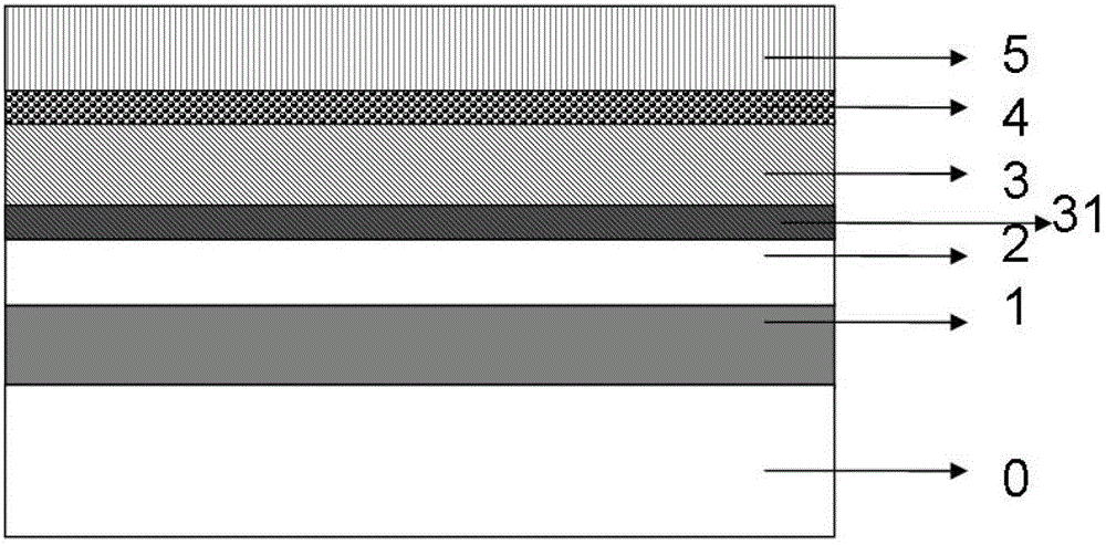
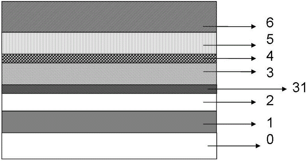
[0031]1) Use MOCVD or MBE to sequentially grow Al(Ga)As substrate peeling laye...


PUM

PropertyMeasurementUnit
thicknessaaaaaaaaaa

Abstract

The invention discloses a method for preparing an inverted-growth wide-spectrum absorption III-V multi-junction cell. Indium phosphide (InP) extension on a gallium arsenide (GaAs) material and monolithic integration of GaAs and InP cells are realized by using a high depth-to-width ratio dislocation capture technology, a GaInP / GaAs / InGaAsP / InGaAs multi-junction cell is prepared on a GaAs substrate by inverted growth, the GaInP / GaAs / InGaAsP / InGaAs multi-junction cell is transferred to a cheap substrate by using a layer transfer technology and a substrate peeling technology, and a high-cost-performance solar cell with high photoelectric conversion efficiency is obtained. The method provided by the invention is easy to implement and low in cost and can be applied to large-scale production of III-V multi-junction solar cells.

Description

technical field [0001] The invention relates to a preparation process of a photovoltaic device, in particular to a preparation method of an inverted growth high-efficiency broad-spectrum absorption III-V multi-junction cell, which belongs to the technical field of solar cells. Background technique [0002] As a typical way of utilizing solar energy, solar cells have become an important development direction of renewable energy. Improving the efficiency of solar cells is one of the goals pursued by solar cells. III-V group compound semiconductors are ideal for solar cell materials due to their broad energy band structure. GaAs-based III-V group multi-junction cells have been the efficiency record holders and creators in the field of solar cells since their inception. According to the solar spectrum and III-V energy band relationship, GaAs-based lattice-matched GaInP / GaAs double-junction cells and InP-based lattice-matched InGaAsP / InGaAs double-junction cells can be reasonably...

Claims


Application Information

Patent Timeline
Patent Type & Authority Applications(China)
IPC IPC(8): H01L31/18
CPCY02P70/50
Inventor 张瑞英董建荣杨辉
Owner SUZHOU INST OF NANO TECH & NANO BIONICS CHINESE ACEDEMY OF SCI
Why Eureka
Try Eureka