
Method for texturing large-area silicon surface in multipoint contact mode

A technology of multi-point contact and processing method, which is applied in the process of producing decorative surface effects, microstructure technology, gaseous chemical plating, etc., can solve the problems of slow processing speed, difficult texture processing, and low efficiency. Achieve the effect of reducing processing cost, reducing operation difficulty and improving processing efficiency

Active Publication Date: 2015-05-20
SOUTHWEST JIAOTONG UNIV
View PDF3 Cites 0 Cited by
  • Summary
  • Abstract
  • Description
  • Claims
  • Application Information

AI Technical Summary

Problems solved by technology

However, this method relies heavily on the ambient humidity and the conductivity of the probe, and the processing environment is very harsh
At the same time, the equipment can only work in single-probe mode, the processing speed is slow and the efficiency is low, and its processing range generally cannot exceed 100 microns, it is difficult to realize large-area texture processing, and it cannot meet the requirements of mass production

Method used


Image

  • Method for texturing large-area silicon surface in multipoint contact mode
  • Method for texturing large-area silicon surface in multipoint contact mode
  • Method for texturing large-area silicon surface in multipoint contact mode

Examples


Embodiment 1

[0025] A large-area silicon surface texturing processing method in a multi-point contact mode, the steps are:

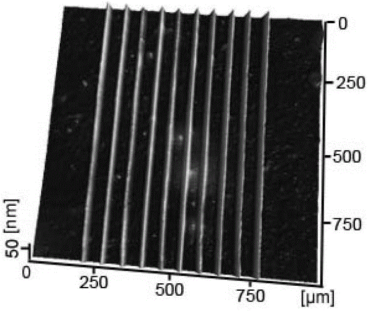
[0026] (1) Place the silicon (100) single wafer at the vertical lower position of the multi-point contact plate, and then make the silicon (100) single wafer and the multi-point contact plate move vertically relative to each other until contact occurs, and reach the set contact load F ; Wherein, the specific composition of the multi-point contact plate is: a plurality of microspheres with a radius of curvature of 160 μm are fixed on the substrate, and the vertices of the plurality of microspheres are on the same plane.

[0027] The contact load F set in this example is 250mN / microsphere. The number of microspheres on the multi-point contact plate is ten, and the material is steel.

[0028] (2) Under the set contact load F, make the multi-point contact plate and the silicon (100) single wafer move relative to each other according to the set track, so that the multi-p...

Embodiment 2

[0033] A large-area silicon surface texturing processing method in a multi-point contact mode, the steps are:

[0034] (1) Place the silicon (100) single wafer at the vertical lower position of the multi-point contact plate, and then make the silicon (100) single wafer and the multi-point contact plate move vertically relative to each other until contact occurs, and reach the set contact load F ; Wherein, the specific composition of the multi-point contact plate is: a plurality of microspheres with a radius of curvature of 160 μm are fixed on the substrate, and the vertices of the plurality of microspheres are on the same plane.

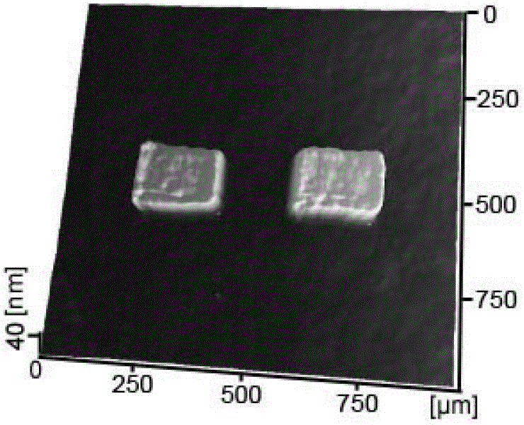
[0035] The contact load F set in this example is 450mN / microsphere. The number of microspheres on the multi-point contact plate is two, and the material is steel.

[0036] (2) Under the set contact load F, make the multi-point contact plate and the silicon (100) single wafer move relative to each other according to the set track, so that the multi-p...

Embodiment 3

[0041] A large-area silicon surface texturing processing method in a multi-point contact mode, the steps are:

[0042] (1) Place the silicon (100) single wafer at the vertical lower position of the multi-point contact plate, and then make the silicon (100) single wafer and the multi-point contact plate move vertically relative to each other until contact occurs, and reach the set contact load F ; Wherein, the specific composition of the multi-point contact plate is: a plurality of microspheres with a radius of curvature of 160 μm are fixed on the substrate, and the vertices of the plurality of microspheres are on the same plane.

[0043] The contact load F set in this example is 250mN / microsphere. The number of microspheres on the multi-point contact plate is seven, and the material is steel.

[0044] (2) Under the set contact load F, make the multi-point contact plate and the silicon (100) single wafer move relative to each other according to the set track, so that the multi...


PUM

PropertyMeasurementUnit
widthaaaaaaaaaa
heightaaaaaaaaaa
lengthaaaaaaaaaa

Abstract

The invention relates to a method for texturing a large-area silicon surface in a multipoint contact mode, which comprises the steps that: a silicon (100) monocrystal slice is arranged under a multipoint contact plate, the silicon slice and the multipoint contact plate are vertically and relatively moved to contact and reach a certain contact load F; the multipoint contact plate and the silicon slice are relatively moved in a set trace, and then etching is performed; after etching, the silicon slice is placed in a KOH solution with the mass factor of 15%-25% and corroded for several minutes, and then a corresponding textured structure with the structure set in advance can be obtained. Because the method is performed in the multipoint contact mode, the pattern, the arrangement mode and the like of the textured structure can be conveniently controlled; and in the etching process, the silicon slice and the multipoint contact plate keep a parallel state all the time. The method has the advantages of low cost of equipment and raw materials, convenience in operation and simple steps, can once complete the processing of large-area textured structure of the silicon (100) monocrystal slice and has the obvious characteristics of low cost and high efficiency.

Description

technical field [0001] The invention relates to a method for processing a surface textured structure, in particular to a method for processing a large-area surface textured silicon chip in a multi-point contact mode. Background technique [0002] Micro / nano technology is the leading industry in the 21st century, and countries around the world regard micro / nano technology as the focus of research and application. When the surface of the material is processed with various textured micro / nano patterns, its light reflection characteristics, friction and wear characteristics, and hydrophilic and hydrophobic characteristics will undergo major changes. This surface texture processing method is widely used in the processing fields of "black silicon" (solar panels with high light absorption rate), hydrophobic bionic materials, engine drag reduction structures, and precision gratings. [0003] Taking silicon, the most important material for micro / nano manufacturing, as an example, th...

Claims


Application Information

Patent Timeline
Patent Type & Authority Patents(China)
IPC IPC(8): B81C1/00
Inventor 钱林茂吴治江余丙军郭剑宋晨飞周仲荣
Owner SOUTHWEST JIAOTONG UNIV
Learn More