
Implementation method and device for full-adder and full-subtractor

A realization method, the technology of the total subtractor, which is applied in the fields of all-optical logic gate, all-optical computing and all-optical communication, can solve problems such as complex structure, and achieve the effect of simple method, easy realization and easy operation

Active Publication Date: 2012-10-17
HUAZHONG UNIV OF SCI & TECH
View PDF1 Cites 0 Cited by
  • Summary
  • Abstract
  • Description
  • Claims
  • Application Information

AI Technical Summary

Problems solved by technology

[0003] So far, all-optical full-adder and full-subtractor are mainly based on cross-gain modulation in semiconductor optical amplifiers (document 1, L.Lei, et.al, "Reconfigurable photonic full-adder and full-subtractor based on three-input XOR gate and logic minterms", Electron.Lett.48, 399, 2012) and the second-order nonlinear effect in periodic polarization inversion lithium niobate (document 2, J.Shen, et.al, "All-Optical Full -Adder Based on Cascaded PPLN Waveguides", J.Quantum Electron.47, 1195, 2011), but their structures are relatively complex, and require four semiconductor optical amplifiers or five periodic polarization inversion lithium niobate cascades

Method used


Image

  • Implementation method and device for full-adder and full-subtractor
  • Implementation method and device for full-adder and full-subtractor
  • Implementation method and device for full-adder and full-subtractor

Examples


example

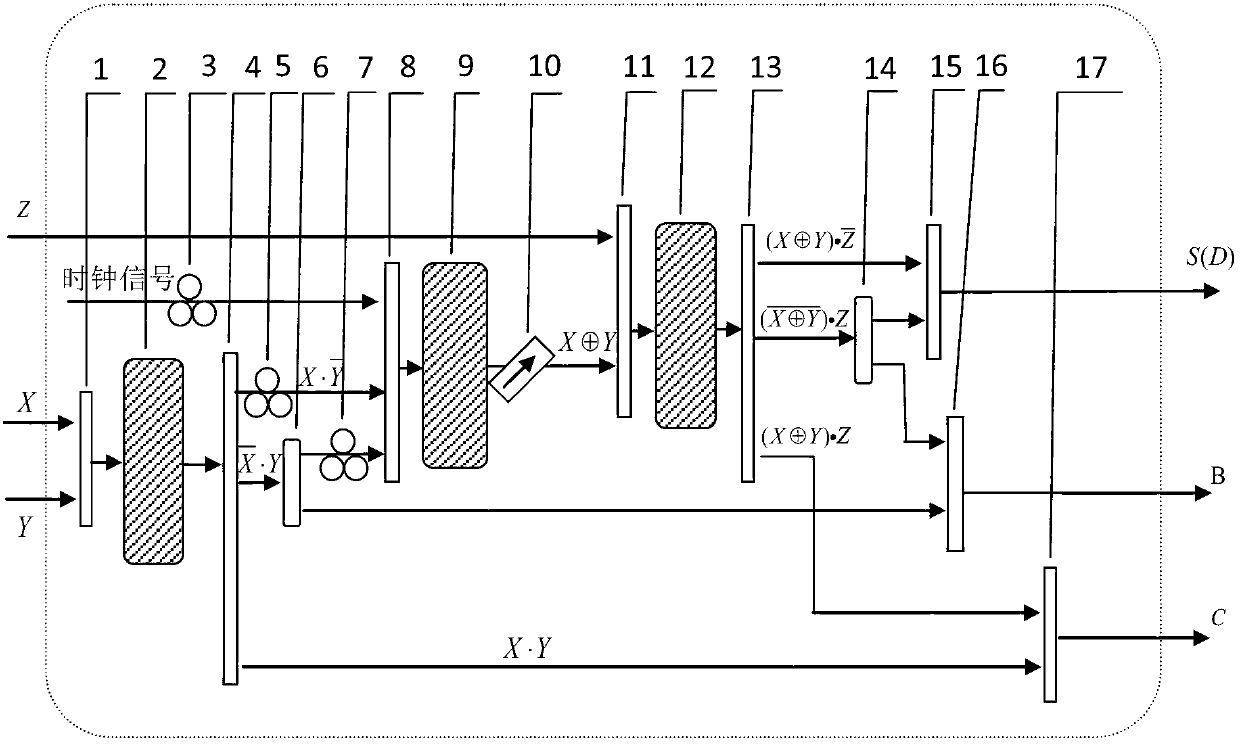
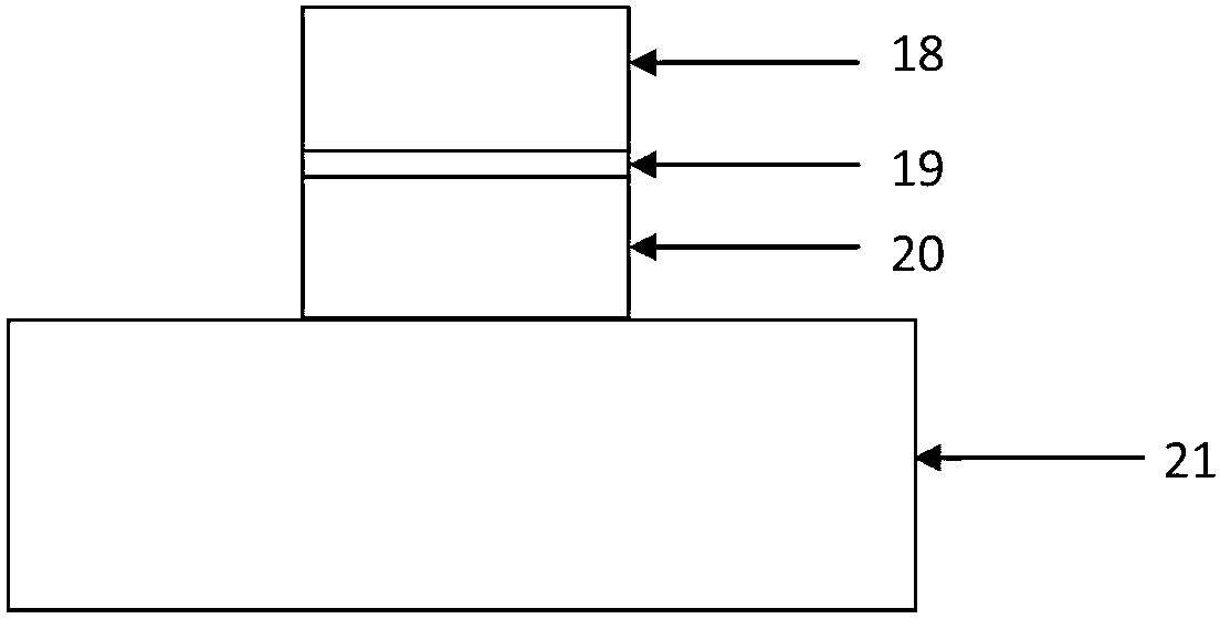
[0037] In this embodiment, the nonlinear waveguides 2, 9, and 12 with third-order nonlinear effects are selected as slot waveguides (the waveguide cross-section is as figure 2 As shown), the length of the three slot waveguides is 5mm, and the width is 250nm. In the cross-sectional structure of the slot waveguide, 18 and 20 are silicon materials with a thickness of 300nm; 19 is a silicon nanocrystalline material with a thickness of 50nm; 21 is The substrate made of silicon dioxide has a thickness of 2 μm.

[0038] When the two input signals of X and Y are input into the first slot waveguide 2, in the waveguide, X and Y will produce a four-wave mixing effect (such as image 3 shown), the optical power of X and Y will be transferred to the two newly generated idler lights, and the optical power of X and Y can be attenuated by selecting appropriate input conditions. After the X signal and Y signal are attenuated, the obtained (wavelength is λ X )with (wavelength is λ Y ) tw...


PUM


Abstract

The invention discloses an implementation method and an implementation device for a full-adder and a full-subtractor. According to the method, three input optical signals are processed by utilizing third-order nonlinear effects in nonlinear waveguides to obtain the output of the full-adder and the full-subtractor. The device comprises first to sixth light wavelength division multiplexers, first to third nonlinear waveguides, first to third polarization controllers, a polarization analyzer, a first light wavelength division multiplexer and a second light wavelength division multiplexer. Compared with other devices for implementing an all-optical full-adder and an all-optical full-subtractor, the device processes three paths of input optical signals by utilizing three nonlinear waveguides to realize the logic operation of full-addition and full-subtraction. Ultra-quick response nonlinear effects are adopted, and the method and the device are applied to the processing and computation of high-speed optical signals. The method and the device are easy to implement, and can work under a high-speed condition. Logic information carried by two wavelengths is converted into a wavelength conversion process of a single wavelength, so that the quality of the signals can be recovered, the extinction ratio of output signals of the full-adder and the full-subtractor can be increased, and the application of the full-adder and the full-subtractor to an optical communication system is facilitated.

Description

technical field [0001] The invention relates to a method and device for realizing full addition and full subtraction logic operations on optical signals, which can be used in the fields of all-optical calculation and all-optical communication, and belongs to the technology in the field of all-optical logic gates. Background technique [0002] In the 21st century, people's demand for information is increasing day by day, and they have higher requirements for network transmission capacity and information processing rate. The all-optical network can provide high-speed and large-capacity transmission and processing capabilities, and can break through the speed bottleneck of the existing network's optical-to-optical conversion. All-optical computing plays an important role in all-optical networks, and all-optical full adders and all-subtractors are key devices for realizing all-optical arithmetic operations, and thus gain more and more attention. [0003] So far, all-optical ful...

Claims


Application Information

Patent Timeline
IPC IPC(8): G02F1/365
Inventor 王健刘勇豪桂成程向超
Owner HUAZHONG UNIV OF SCI & TECH
Learn More