Method for preparing semiconductor material through ion injection and fixed-point adsorption technologies

An ion implantation and semiconductor technology, which is applied in semiconductor/solid-state device manufacturing, electrical components, circuits, etc., can solve problems such as process instability and difficulty in achieving low defect density, and achieve reduced process difficulty, low defect density, and increased stability Effect

Active Publication Date: 2015-03-18
SHANGHAI INST OF MICROSYSTEM & INFORMATION TECH CHINESE ACAD OF SCI
View PDF5 Cites 0 Cited by
  • Summary
  • Abstract
  • Description
  • Claims
  • Application Information

AI Technical Summary

Problems solved by technology

[0006] In view of the shortcomings of the prior art described above, the object of the present invention is to provide a method for preparing semiconductor materials using ion implantation and fixed-point adsorption processes, which is used to solve the unstable process of preparing relaxed SiGe materials by ion implantation processes in the prior art. However, it is difficult to realize the preparation of SiGe with low defect density and high relaxation degree.

Method used


Image

  • Method for preparing semiconductor material through ion injection and fixed-point adsorption technologies
  • Method for preparing semiconductor material through ion injection and fixed-point adsorption technologies
  • Method for preparing semiconductor material through ion injection and fixed-point adsorption technologies

Examples


Embodiment 1

[0043] like Figure 1~Figure 9 As shown, this embodiment provides a method for preparing semiconductor materials using ion implantation and fixed-point adsorption processes, which at least includes the following steps:

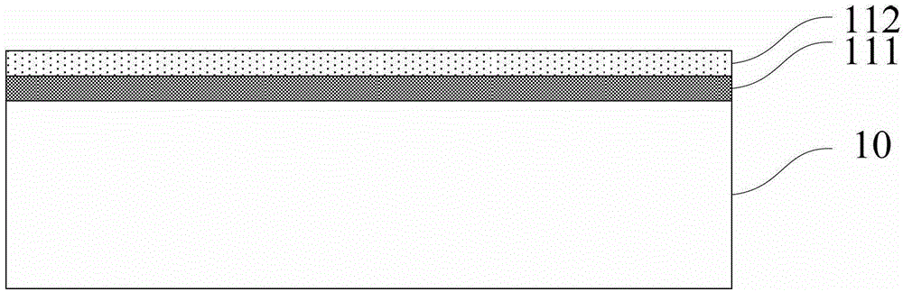
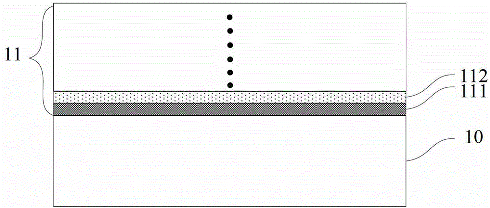
[0044] like Figure 1~Figure 2 As shown, step 1) is firstly performed to provide a first Si substrate 10, and Si substrates are alternately formed on the surface of the Si substrate. x Ge 1-x layer 111 and Si layer 112, forming at least one period of Si x Ge 1-x / Si superlattice structure 11, where 0≤x<1.

[0045] The Si x Ge 1-x The thicknesses of the layer 111 and the Si layer 112 are both 1-10 nm. In this embodiment, three periods of Si are formed on the surface of the first Si substrate 10 by chemical vapor deposition. x Ge 1-x / Si, wherein, x is 0.9, 0.8, 0.7 according to the order of formation, and the Si x Ge 1-x Both the layer 111 and the Si layer 112 have a thickness of 8 nm. Of course, in its embodiment, the Si x Ge 1-x The period numbe...

Embodiment 2

[0060] like Figure 10~Figure 19 As shown, this embodiment provides a method for preparing semiconductor materials using ion implantation and fixed-point adsorption processes, such as Figure 10~16As shown, its steps 1)~step 3) are as step 1)~step 3) in embodiment 1, the subsequent steps of this embodiment are:

[0061] like Figure 17 shown, proceed to step 4), where the relaxed Si z Ge 1-z A strained Si layer 18 is formed on the surface of the layer 15, and the thickness of the strained Si layer 18 is less than its critical thickness.

[0062] The strained Si layer 18 is formed by chemical vapor deposition, since the relaxed Si z Ge 1-z Layer 15 has the characteristics of low defect density and high relaxation, so the Si layer grown on it has the characteristics of high strain and low defect density.

[0063] like Figure 18 As shown, proceed to step 5), providing a second Si substrate 17 with an oxide layer 16 on the surface, and bonding the oxide layer 16 and the st...


PUM

PropertyMeasurementUnit
thicknessaaaaaaaaaa
thicknessaaaaaaaaaa

Abstract

The invention provides a method for preparing a semiconductor material through ion injection and fixed-point adsorption technologies. The method comprises the steps of firstly extending at least one period of an SixGe1-x / Si superlattice structure (x is greater than or equal to 0 and smaller than 1) on an Si substrate, sequentially growing an Si buffer layer and an SizGe1-z layer on the superlattice structure, then injecting H or He ions into the Si substrate and performing rapid annealing treatment, so as to ensure that the superlattice structure is adsorbed to the ions, and finally obtaining an SizGe1-z layer with low defect concentration and high relaxation. By bonding with the Si substrate with an oxidation layer, SGOI with low defect concentration and high relaxation can be prepared through smart cut, strained silicon with the thickness being smaller than the critical thickness is expanded on the obtained relaxation SizGe1-z layer, and strained silicon (sSOI) with high relaxation and low defect concentration on insulators can be prepared through smart cut. The method improves the stability of relaxation SiGe material prepared through ion injection through superlattice adion, obtains SiGe material with low defect concentration and high relaxation, reduces the technology difficulty, and is applicable to industrial production.

Description

technical field [0001] The invention belongs to the field of semiconductors, in particular to a method for preparing semiconductor materials by using ion implantation and fixed-point adsorption techniques. Background technique [0002] According to the planning of the International Semiconductor Industry Development Blueprint (ITRS2009), integrated circuits have gradually developed from the era of microelectronics to the era of micro-nanoelectronics. The existing bulk silicon materials and processes are approaching their physical limits and have encountered severe challenges. SOI has become the mainstream technology of deep submicron low-voltage, low-power integrated circuits. SOI (Silicon-On-Insulator, silicon on insulating substrate) technology introduces a buried oxide layer between the top silicon and the back substrate. By forming a semiconductor thin film on an insulator, the SOI material has the incomparable advantages of bulk silicon: it can realize the dielectric i...

Claims


Application Information

Patent Timeline
Patent Type & Authority Patents(China)
IPC IPC(8): H01L21/20H01L21/02H01L21/324
Inventor 张苗母志强薛忠营陈达狄增峰王曦
Owner SHANGHAI INST OF MICROSYSTEM & INFORMATION TECH CHINESE ACAD OF SCI
Why Eureka
Try Eureka