A kind of double polycrystalline soi SiGe HBT integrated device and preparation method based on self-alignment process

A self-aligned process and integrated device technology, which is applied in semiconductor/solid-state device manufacturing, electrical solid-state devices, semiconductor devices, etc., and can solve the problems of lack of wide application and development, incompatibility of Si process, and more complicated preparation process than Si process.

Inactive Publication Date: 2015-08-12
XIDIAN UNIV
View PDF3 Cites 0 Cited by
  • Summary
  • Abstract
  • Description
  • Claims
  • Application Information

AI Technical Summary

Problems solved by technology

[0006] The purpose of the embodiments of the present invention is to provide a dual-polycrystalline SOI SiGeHBT integrated device based on self-alignment technology and its preparation method, aiming at solving the problem that although GaAs and InP-based compound devices have superior frequency characteristics, their preparation process is more complex than Si process, High cost, difficult preparation of large diameter single crystal, low mechanical strength, poor heat dissipation performance, difficult compatibility with Si process and lack of SiO 2 Such passivation layer and other factors limit its wide application and development

Method used


Image

  • A kind of double polycrystalline soi SiGe HBT integrated device and preparation method based on self-alignment process
  • A kind of double polycrystalline soi SiGe HBT integrated device and preparation method based on self-alignment process
  • A kind of double polycrystalline soi SiGe HBT integrated device and preparation method based on self-alignment process

Examples


Embodiment 1

[0075] Embodiment 1: The method for preparing a double-polycrystalline SOI SiGe HBT integrated device and circuit with a base thickness of 20nm by using a self-alignment process provided, the specific steps are as follows:

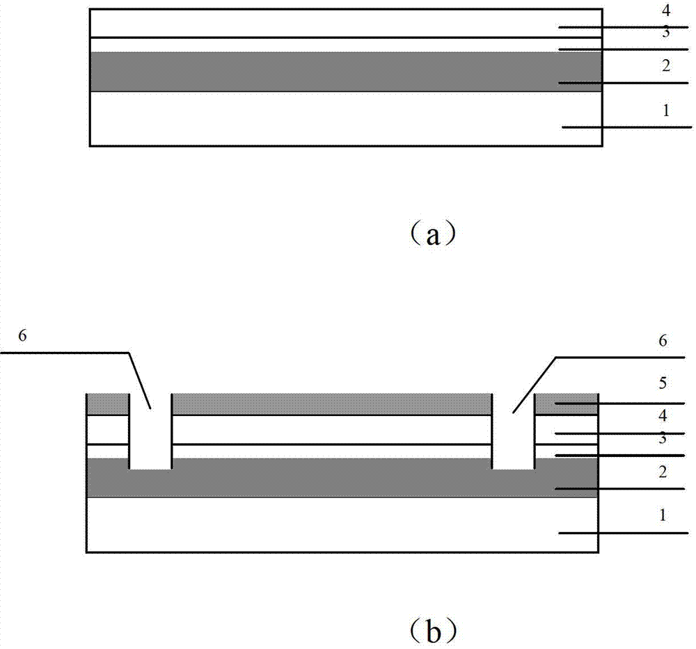
[0076] Step 1, epitaxial growth, such as figure 2 (a) shown.

[0077] (1a) Select the SOI substrate sheet, the support material 1 of the lower layer of the substrate is Si, and the intermediate layer 2 is SiO 2 , the thickness is 150nm, and the upper layer material 3 has a doping concentration of 1×10 16 cm -3 N-type Si with a thickness of 100nm;

[0078] (1b) Using the chemical vapor deposition (CVD) method, at 600 ° C, grow a layer of N-type epitaxial Si layer 4 with a thickness of 50 nm on the upper Si material, as the collector region, and the doping concentration of this layer is 1 ×10 16 cm -3 .

[0079] Step 2, shallow trench isolation preparation, such as figure 2 (b), (c) shown.

[0080] (2a) Deposit a layer of SiO with a thickness of 3...

Embodiment 2

[0109] Embodiment 2: The method for preparing a double-polycrystalline SOISiGeHBT integrated device and circuit with a base thickness of 40 nm by using a self-alignment process is provided, and the specific steps are as follows:

[0110] Step 1, epitaxial growth, such as figure 2 (a) shown.

[0111] (1a) Select the SOI substrate sheet, the support material 1 of the lower layer of the substrate is Si, and the intermediate layer 2 is SiO 2 , the thickness is 300nm, and the upper material 3 has a doping concentration of 5×10 16 cm -3 N-type Si with a thickness of 120nm;

[0112] (1b) Using the chemical vapor deposition (CVD) method, at 700 ° C, grow an N-type epitaxial Si layer 4 with a thickness of 80 nm on the upper Si material as the collector region, and the doping concentration of this layer is 5 ×10 16 cm -3 .

[0113] Step 2, shallow trench isolation preparation, such as figure 2 (b), (c) shown.

[0114] (2a) Deposit a layer of SiO with a thickness of 400nm on t...

Embodiment 3

[0143] Embodiment 3: The method for preparing a dual-polycrystalline SOI SiGeHBT integrated device and circuit with a base thickness of 60 nm by using a self-alignment process is provided, and the specific steps are as follows:

[0144] Step 1, epitaxial growth, such as figure 2 (a) shown.

[0145] (1a) Select the SOI substrate sheet, the support material 1 of the lower layer of the substrate is Si, and the intermediate layer 2 is SiO 2 , the thickness is 400nm, and the upper material 3 has a doping concentration of 1×10 17 cm -3 N-type Si with a thickness of 150nm;

[0146] (1b) Using the chemical vapor deposition (CVD) method, at 750 ° C, grow a layer of N-type epitaxial Si layer 4 with a thickness of 100 nm on the upper Si material, as the collector region, and the doping concentration of this layer is 1 ×10 17 cm -3 .

[0147] Step 2, shallow trench isolation preparation, such as figure 2 (b), (c) shown.

[0148] (2a) Deposit a layer of SiO with a thickness of 5...


PUM


Abstract

The invention is suitable for the technical field of semiconductor integrated circuit and provides a double-polysilicon SOI (Silicon On Insulator) SiGe HBT (Heterojunction Bipolar Transistor) integrated device based on self-aligned technology and a preparation method thereof. The preparation method comprises the following steps: growing N-type Si epitaxy on an SOI substrate; photoetching a shallow slot isolation region; preparing shallow slot isolation; etching and injecting phosphonium ions to form a collector contact region; depositing SiO2, P-Poly-Si, SiO2 and nitride in sequence; carrying out dry etching to form a nitride side wall; carrying out wet etching to form a base region window; selectively growing a SiGe base region; depositing N-type Poly-Si; then removing Poly-Si outside an emitter to form an HBT (Heterojunction Bipolar Transistor); and finally photoetching an emitter region, the base region and a collector region pin hole, metalizing, photoetching a lead wire to form an HBT integrated circuit in which the thickness of the base region is 20-60nm. The technique provided by the invention is compatible with the existing CMOS (Complementary Metal-Oxide-Semiconductor) integrated circuit processing technology, and can prepare the integrated circuit of a BiCMOS (Bipolar-Complementary Metal-Oxide-Semiconductor) device based on SOI under the condition of little capital and equipment investment so that the performance of the existing analog and digital-analog hybrid integrated circuit is greatly improved.

Description

technical field [0001] The invention belongs to the technical field of semiconductor integrated circuits, and in particular relates to a double-polycrystalline SOI SiGe HBT integrated device and a preparation method based on a self-alignment process. Background technique [0002] Integrated circuits are the cornerstone and core of the economic development of an information society. Just as the American engineering and technology circle recently named the fifth electronic technology among the 20 greatest engineering and technological achievements in the world in the 20th century, "from vacuum tubes to semiconductors and integrated circuits, they have become the cornerstone of intelligent work in various industries today." Integrated circuits. It is one of the typical products that can best reflect the characteristics of knowledge economy. At present, the electronic information industry based on integrated circuits has become the world's largest industry. With the developmen...

Claims


Application Information

Patent Timeline
Patent Type & Authority Patents(China)
IPC IPC(8): H01L27/12H01L21/84
Inventor 胡辉勇宋建军王斌张鹤鸣宣荣喜王海栋周春宇郝跃
Owner XIDIAN UNIV
Why Eureka
Try Eureka