

Waveguide mode-locked laser
A mode-locked laser and waveguide grating technology, applied in the field of lasers, can solve the problems of reducing the high integration of waveguide mode-locked lasers and technical barriers to optical integration, etc.
- Summary
- Abstract
- Description
- Claims
- Application Information
AI Technical Summary
Problems solved by technology
Method used
Image

Examples
Embodiment Construction
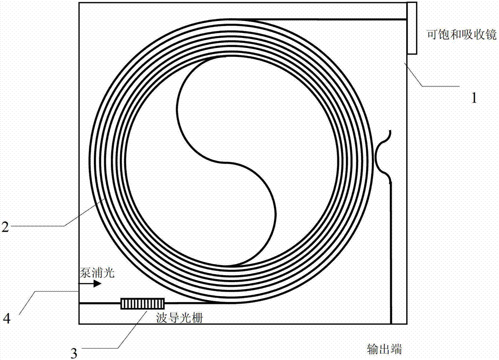
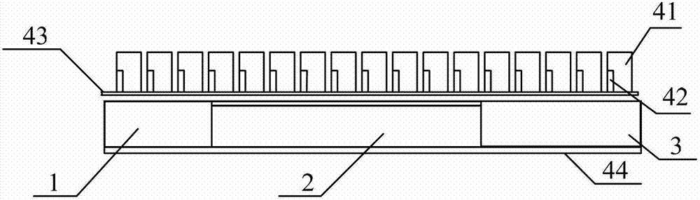
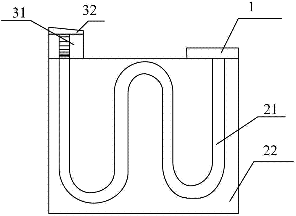
[0019] see figure 1 , the waveguide mode-locked laser of the present invention is mainly composed of 4 parts, a semiconductor saturable absorbing mirror 1, a waveguide gain medium 2, a waveguide grating 3, a laser diode array pump source 4; a semiconductor saturable absorbing mirror 1 and a waveguide grating 3 are respectively arranged at both ends of the waveguide gain medium 2, and the laser diode array pump source 4 is arranged on the waveguide grating. The semiconductor saturable absorbing mirror 1 is fixed to the output end of the waveguide gain medium 2 through a precision control platform, and the semiconductor saturable absorbing mirror 1 is fixed with special glue, thereby realizing the saturable absorbing mirror 1 It is integrated with the waveguide to meet the structure of the whole waveguide.
[0020] see figure 2 , image 3 , the waveguide gain medium 2 is a piece of doped material with a thickness of 220 μm, a width of 11 mm, and a length of 60 mm. The bottom...
PUM
 Abstract
Description
Claims
Application Information