Anti-radiation complementary metal oxide semiconductor (CMOS) device and preparation method thereof

A device and vertical channel technology, which is applied in the radiation-resistant CMOS device and its preparation field, can solve the problems of a single radiation resistance index and does not consider the small-size charge sharing effect, so as to improve the characteristics of single particles, improve the charge sharing effect, Effect of Improving Dosage Characteristics

Inactive Publication Date: 2012-11-07
PEKING UNIV
View PDF5 Cites 13 Cited by
  • Summary
  • Abstract
  • Description
  • Claims
  • Application Information

AI Technical Summary

Problems solved by technology

However, these new device structures often can only achieve a single radiation resistance index, and cannot simultaneously meet the requirements of both total dose radiation resistance and single event radiation resistance, and at the same time, the charge sharing effect caused by small size is not considered.

Method used


Image

  • Anti-radiation complementary metal oxide semiconductor (CMOS) device and preparation method thereof
  • Anti-radiation complementary metal oxide semiconductor (CMOS) device and preparation method thereof
  • Anti-radiation complementary metal oxide semiconductor (CMOS) device and preparation method thereof

Examples


Embodiment Construction

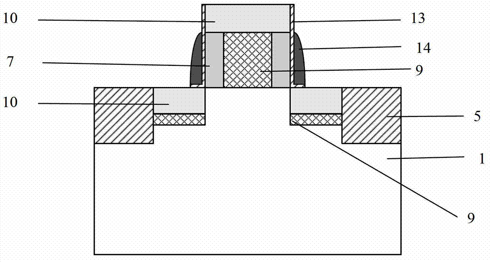
[0024] The embodiments of the present invention will be described in detail below by taking NMOS as an example with reference to the accompanying drawings, wherein the material of the dielectric protection area is silicon nitride.

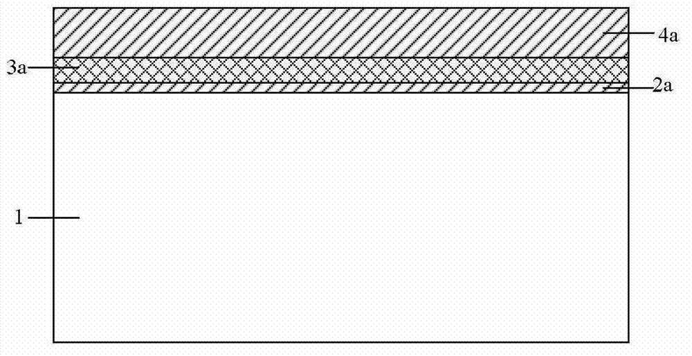
[0025] 1) Preparation: prepare P-type (100) silicon substrate 1;

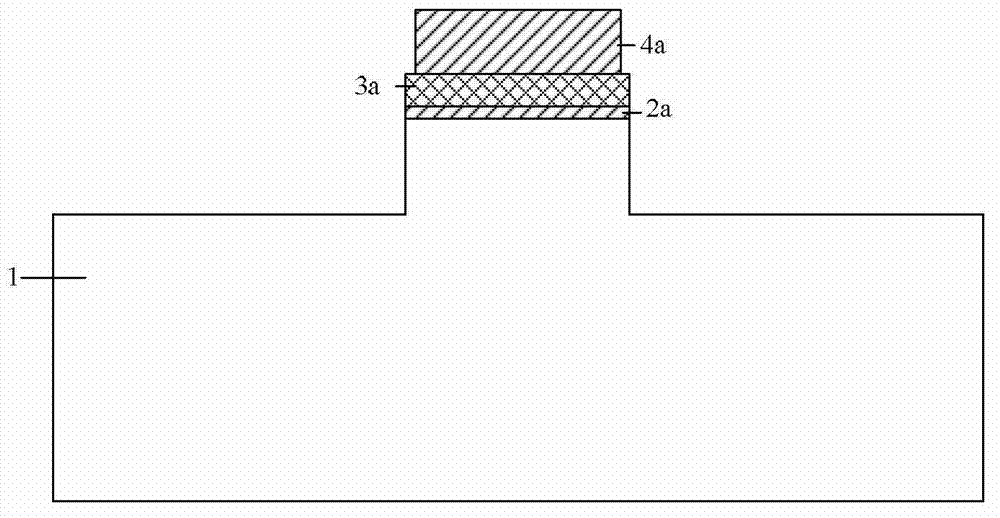
[0026] 2) Etching the active area silicon stage: first thermally oxidize a thin layer of silicon dioxide 2a on the substrate, then low-pressure chemical vapor deposition (LPCVD) a layer of silicon nitride 3a, and then LPCVD a layer of silicon dioxide 4a, such as Figure 2(a); photolithography, reactive ion etching (RIE) silicon dioxide 4a, RIE etching silicon nitride 3a, hydrofluoric acid etching silicon dioxide 2a, so that the etched silicon dioxide 4a and nitride There are tiny steps between the silicon 3a; inductively coupled plasma (ICP) etches the silicon substrate 1 to form a silicon mesa in the active region, as shown in Figure 2(b);

[0027] 3) Form the device isolation regi...


PUM


Abstract

The invention discloses an anti-radiation complementary metal oxide semiconductor (CMOS) device and a preparation method thereof and belongs to the technical field of CMOS integrated circuit. The CMOS device comprises a substrate, a source region, a drain region and a vertical channel located on the substrate. A first medium protective region is added in the vertical channel, the first medium protective region is located in the middle of the vertical channel to separate the vertical channel into two portions, the height of the first medium protective region is equal to the length of the vertical channel, an active silicon platform central axis serves as a center, and the distance between the edge of the first medium protective region and the outside of the channel is 20-100nm. Simultaneously a second medium protective region is arranged below the source region or the drain region on the substrate, the length of the second medium protective region is equal to that of the source region or the drain region, and the height of the second medium protective region is 10-50nm. The medium protective regions are added, a route of the source region and the drain region for collecting charges can be effectively separated, and signal grain characteristics of the device are improved.

Description

technical field [0001] The invention belongs to the technical field of CMOS integrated circuits, and in particular relates to a radiation-resistant CMOS device and a preparation method thereof. Background technique [0002] The rapid development and wide application of information technology has changed the traditional production, operation, management and way of life, and has brought a profound impact on all aspects of human society. With the development of science and technology, especially the development of space technology, nuclear power and nuclear weapons, the relationship between nuclear radiation environment and electronic technology is getting closer and closer. In order to meet the requirements of the development of aerospace technology for the radiation resistance of integrated circuits, some key core integrated circuits of satellites and spacecraft need to use radiation resistance hardened devices. Therefore, the development of the aerospace industry and the pr...

Claims


Application Information

Patent Timeline
Patent Type & Authority Applications(China)
IPC IPC(8): H01L27/092H01L29/78H01L23/552H01L21/8238
CPCH01L21/823828H01L21/823885H01L21/823814H01L27/092H01L29/66636H01L29/66666H01L29/7827H01L21/8238H01L29/7788
Inventor 黄如谭斐安霞武唯康黄良喜
Owner PEKING UNIV
Why Eureka
Try Eureka