
Chemical nickel-plating method for capacitive touch screen indium tin oxide (ITO) wiring

A capacitive touch screen, chemical nickel plating technology, applied in liquid chemical plating, metal material coating process, coating and other directions, can solve the problem of fast etching of ITO film, poor coating adhesion, weak sensitization solution selectivity, etc. problem, to achieve the effect of operation spirituality, low cost and fast production speed

Inactive Publication Date: 2012-11-14
NANJING UNIV OF AERONAUTICS & ASTRONAUTICS
View PDF8 Cites 8 Cited by
  • Summary
  • Abstract
  • Description
  • Claims
  • Application Information

AI Technical Summary

Problems solved by technology

However, the selectivity of the sensitizing solution used in these methods in electroless nickel plating is weak, and it is easy to adsorb on the glass substrate while adsorbing on ITO, which leads to the complexity of the subsequent process; at the same time, the traditional etching solution contains MnO 4 - , it etches the ITO film too fast, it is difficult to control, and the etched micropit aperture is too large, it is easy to make the ITO film non-conductive or locally non-conductive; in addition, the traditional acidic electroless nickel plating process has a plating temperature of 75 ~90°C, may cause poor adhesion between coatings

Method used


Image

  • Chemical nickel-plating method for capacitive touch screen indium tin oxide (ITO) wiring
  • Chemical nickel-plating method for capacitive touch screen indium tin oxide (ITO) wiring
  • Chemical nickel-plating method for capacitive touch screen indium tin oxide (ITO) wiring

Examples


Embodiment 1

[0040] Embodiment 1 Electroless nickel plating is performed as follows:

[0041] (1) Degreasing: Put the glass substrate with ITO film into the ethanol solution for 3-5 minutes and put the glass substrate that has been sonicated in ethanol into the alkaline degreasing solution (the formula is 15g / L NaOH, 20g / L Na of L 3 PO 4, 20g / L Na 2 CO 3 , 10g / L sodium silicate, 3g / L OP emulsifier) ​​for ultrasonic degreasing for 10 minutes, then rinse with deionized water;

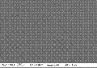
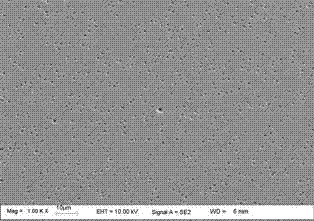
[0042] (2) Etching: Put the degreased ITO thin film glass into the etching solution (the formula is 50g / L KHS 2 o 8 , 40g / L Na 2 SO 4 , 1mL / L concentrated H 2 SO 4 , 4g / L NH 4 HF 2 , 15g / L citric acid), coarsened at 30°C for 5 minutes, then put the ITO glass into deionized water and ultrasonicated for 1 minute; its morphology is shown in figure 2 ;

[0043] (3) Sensitization: Put the etched ITO thin film glass into self-made sensitization solution A (see Table 1) and sensitize it at 30°C for 6 minutes, t...

Embodiment 2

[0050] Embodiment 2 is different from Embodiment 1 in following 4 steps:

[0051] (2) Etching: The difference from Example 1 is that the etching solution formula is 50g / L KHS 2 o 8 , 40g / L Na 2 SO 4 , 1.5mL / L concentrated H 2 SO 4 , 4g / L NH 4 HF 2 , 15g / L citric acid, roughening time is 8 minutes;

[0052] (3) Sensitization: the difference from Example 1 is that the sensitization time is 7 minutes;

[0053] (4) Activation: The difference from Example 1 is that the formula of the activation solution is 0.2g / L PdCl 2 , 3mL / L concentrated HCl; its morphology after the subsequent reduction operation is shown in Figure 4 , see the energy spectrum Figure 5 ;

[0054] (6) Electroless nickel plating: The difference from Example 1 is that electroless plating is carried out in an acidic bath with a pH of 4.7, and its topography is shown in Figure 7 .

[0055] After this step, the ITO thin film is electroless nickel-plated, and the analysis spectrum shows that:

[0056] ...

Embodiment 3

[0059] Embodiment 3 is different from Embodiment 1 in following 4 steps:

[0060] (2) Etching: The difference from Example 1 is that the etching solution formula is 40g / L KHS 2 o 8 , 40g / L Na 2 SO 4 , 1.5mL / L concentrated H 2 SO 4 , 4g / L NH 4 HF 2 , 15g / L citric acid, the roughening time is 8 minutes, its appearance is shown in image 3 ;

[0061] (3) Sensitization: The difference from Example 1 is that the sensitization time is 8 minutes;

[0062] (4) Activation: The difference from Example 1 is that the formula of the activation solution is 0.3g / L PdCl 2 , 5mL / L concentrated HCl; the activation time is 8 minutes;

[0063] (6) Electroless nickel plating: The difference from Example 1 is that electroless plating is carried out in an acidic bath with pH 5.0, and its topography is shown in Figure 8 .

[0064] After this step, the ITO thin film is electroless nickel-plated, and the analysis spectrum shows that:

[0065] 1. by image 3 (After etching) you can see th...


PUM


Abstract

The invention provides a novel chemical nickel-plating method for capacitive touch screen indium tin oxide (ITO) wiring. Compared with the conventional vacuum sputtering technology, the novel chemical nickel-plating method is low in equipment investment, low in production cost and high in efficiency; and compared with the traditional chemical nickel-plating process on a nonmetallic matrix, the novel chemical nickel-plating method has high solution stability and selectivity. The novel chemical nickel-plating method comprises the following steps of: sequentially deoiling, etching, sensitizing, activating, reducing and performing chemical nickel-plating on the ITO film glass; and the key points are that the selectivity of the ITO film is improved during sensitization by adopting sensitizing solution containing Cu+, and the sensitizing solution is more stable than the traditional Sn2+ sensitizing solution; during etching, the etching process is stabilized by employing etching solution containing S2O82- or HS2O8-, and the etching effect is improved; and the chemical nickel-plating is performed at the low temperature of 55-65 DEG C, the plating solution is stable, and the plating layer is smooth and dense. The results prove that the method is easy to operate and high in speed; the ITO surface nickel layer is completely covered and has high adhesive force, and the glass matrix is not covered by the nickel layer and has high selectivity.

Description

technical field [0001] The invention belongs to the technical field of capacitive touch screen ITO surface plating, and in particular relates to an electroless nickel plating method used on the ITO wiring of a capacitive touch screen. Background technique [0002] Tin-doped indium oxide (Indium Tin Oxide, referred to as ITO) thin film is a semiconductor material with excellent photoelectric properties and conductivity, so it has developed rapidly in recent years, especially in the manufacture of thin-film transistors (TFT), flat-panel liquid crystal displays (LCDs) ), electronic products such as touch-screen mobile phones and computers have been widely used, forming a certain market size. After sputtering ITO on the surface of the capacitive touch screen glass substrate, it becomes a double-sided ITO glass. The ITO films on different sides need to be connected through the ITO wires on the four edges. In order to reduce the input impedance limit of the control chip, it is nec...

Claims


Application Information

Patent Timeline
IPC IPC(8): C23C18/32C23C18/18
Inventor 梅天庆任春春
Owner NANJING UNIV OF AERONAUTICS & ASTRONAUTICS
Learn More