Induction gate type amorphous metal oxide TFT gas sensor
An amorphous oxide and gas sensor technology, applied in the direction of transistors, semiconductor devices, electrical components, etc., to achieve the effect of online active amplification signal changes, high sensitivity and large area
- Summary
- Abstract
- Description
- Claims
- Application Information
AI Technical Summary
Problems solved by technology
Method used
Image

Examples
Embodiment 1
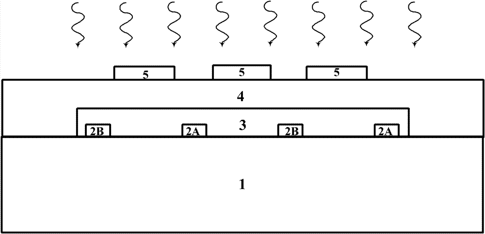
[0039] Such as Figure 1A Shown is a schematic diagram of an induction gate TFT gas sensor according to the present invention, including a substrate 1 , source and drain electrodes 2 , a TFT conductive film 3 , a gate insulating dielectric layer 4 , and a top gate electrode 5 . Wherein, the substrate 1 is an insulating substrate and provides support, and its material is, for example, a silicon chip whose surface is an insulating layer (preferably silicon-on-insulator SOI, or it can be deposited on a bulk silicon substrate or thermally oxidized to make silicon dioxide. The liner layer can also form an insulating layer of silicon nitride or silicon oxynitride on the bulk silicon), glass (can be doped as commonly used borophosphosilicate glass BPSG, or spin-on-glass SOG, and the glass substrate 1 is preferably It has a rectangular shape for cutting and large-area fabrication), quartz, plastic (preferably a composition with a higher melting point and hardness and good insulation), ...
Embodiment 2
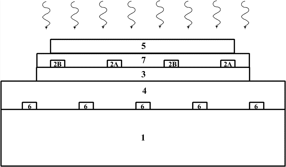
[0049] Such as Figure 2A Shown is a schematic cross-sectional view of an induction gate TFT gas sensor according to the present invention, including. Wherein, the back gate electrode 6 is formed by sputtering deposition first on the substrate 1 such as a silicon wafer with an insulating layer on the surface, a silicon wafer substrate with a hollowed out back, glass, quartz, plastic, etc., and its material is, for example, Mo, Pt, Al, Ti, Co, Au, Cu, etc. can also be other materials with conductive function, such as doped polysilicon, such as metal nitrides such as TiN and TaN, and the like. Subsequently, a gate insulating dielectric layer 4 is formed on the substrate 1 and the back gate electrode 6, for example, silicon dioxide, silicon nitride, silicon oxynitride, or high-k materials such as hafnium oxide and tantalum oxide are deposited by low-temperature CVD. , can also be a combination of these materials, and the combination can be mixed or laminated. On the gate insula...
PUM
| Property | Measurement | Unit |
|---|---|---|
| Thickness | aaaaa | aaaaa |
Abstract
Description
Claims
Application Information
 - Generate Ideas
- Intellectual Property
- Life Sciences
- Materials
- Tech Scout
- Unparalleled Data Quality
- Higher Quality Content
- 60% Fewer Hallucinations
Browse by: Latest US Patents, China's latest patents, Technical Efficacy Thesaurus, Application Domain, Technology Topic, Popular Technical Reports.
© 2025 PatSnap. All rights reserved.Legal|Privacy policy|Modern Slavery Act Transparency Statement|Sitemap|About US| Contact US: help@patsnap.com