Manufacture method of thin film transistor and with indium zinc aluminum oxide as channel layer

A technology of indium zinc aluminum oxide and thin film transistors, which is applied in semiconductor/solid-state device manufacturing, electrical components, circuits, etc., can solve the problem of large off-state current of devices, and achieve the effect of simple process and low cost

Inactive Publication Date: 2012-11-14
FUDAN UNIV
View PDF5 Cites 6 Cited by
  • Summary
  • Abstract
  • Description
  • Claims
  • Application Information

AI Technical Summary

Problems solved by technology

Usually, the carrier concentration of the IZO system is too hi

Method used


Image

  • Manufacture method of thin film transistor and with indium zinc aluminum oxide as channel layer
  • Manufacture method of thin film transistor and with indium zinc aluminum oxide as channel layer
  • Manufacture method of thin film transistor and with indium zinc aluminum oxide as channel layer

Examples


Embodiment 1

[0030] Among the present invention, PMMA solid powder is purchased from Sigma-Aldrich company, and molecular weight is 12000.

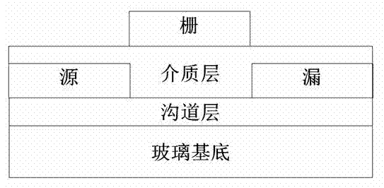
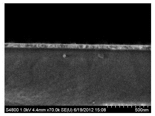
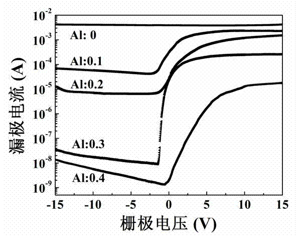
[0031] First, an indium zinc aluminum oxide film is prepared on a glass substrate as a channel layer. The specific implementation is: using ethanolamine as a stabilizer (wherein, the volume ratio of ethanolamine to ethylene glycol is 0.1:20), the analytically pure In(NO 3 ) 3 4.5H 2 O, Zn(C 2 h 3 o 2 ) 2 ·5H 2 O and AlCl 3 ·6H 2 O is dissolved in ethylene glycol and stirred at 60°C for 1 hour to form a clear and transparent precursor solution. When the precursor solution ([Al 3+ ]+ [In 3+ ]+[Zn 2+ ]) at a concentration of 0.25 M, the molar ratio of indium to zinc (In 3+ : Zn 2+ ) under the premise of 1:1, the prepared aluminum molar content is [Al] 3+ / ([In 3+ ]+[Zn 2+ ]) = 0, 0.1, 0.2 , 0.3, 0.4 of the precursor solution. After the prepared solution was left to age for 48 hours, the glass substrate was dipped for pulling coating. Af...


PUM

PropertyMeasurementUnit
Thicknessaaaaaaaaaa

Abstract

The invention belongs to the technical field of thin film transistors and particularly relates to a manufacture method of a thin film transistor and with indium zinc aluminum oxide as a channel layer. The method utilizes aluminum to be mingled with indium zinc aluminum oxide to obtain an indium zinc aluminum oxide semiconductor film and improve performance of the channel layer of an indium zinc aluminum oxide semiconductor. The manufacture method utilizes the impregnation pulling method process which is low in cost, simple in process, easy to prepare in large area to prepare an indium zinc aluminum oxide thin film which is smooth in surface and even and compact in thickness, and the indium zinc aluminum oxide thin film is applied to manufacture of oxide thin film transistors. A manufactured thin film transistor device is good in comprehensive performance and has high saturation migration rate which is 26.8cm<2>/Vs and low subthreshold amplitude which is 0.24V/decade. The switch ratio is larger than 104.

Description

technical field [0001] The invention belongs to the technical field of thin film transistors, and in particular relates to a preparation method of a thin film transistor using indium zinc aluminum oxide as a channel layer. Background technique [0002] Thin film transistor (TFT) is a core component in active driving, which includes several important components such as substrate, semiconductor channel layer, dielectric layer, gate, source and drain. At present, the most widely used and mature technology in the display field is the TFT prepared by using silicon material as the semiconductor channel layer. With the improvement of people's demand, and in order to break through the saturated LCD market, it is necessary to realize a new generation of display technologies such as 3D display, transparent display and flexible display. Facing the new generation of display technology, traditional silicon-based TFTs show some shortcomings. At present, transparent amorphous oxide semic...

Claims


Application Information

Patent Timeline
IPC IPC(8): H01L21/336
Inventor 岳兰张群
Owner FUDAN UNIV
Why Eureka
Try Eureka