
ESD (Electronic Static Discharge) protection structure based on partial depletion mode SOI (Silicon on Insulator) process

An ESD protection and depletion-type technology, which is applied in the direction of electrical components, electric solid-state devices, circuits, etc., can solve the problems that it is difficult to meet the diverse needs of input/output ports, so as to improve the ESD tolerance level, simple structure, and easy to use. convenient effect

Active Publication Date: 2012-11-14
58TH RES INST OF CETC
View PDF8 Cites 3 Cited by
  • Summary
  • Abstract
  • Description
  • Claims
  • Application Information

AI Technical Summary

Problems solved by technology

The above two methods are difficult to meet the diverse needs of input / output ports

Method used


Image

  • ESD (Electronic Static Discharge) protection structure based on partial depletion mode SOI (Silicon on Insulator) process
  • ESD (Electronic Static Discharge) protection structure based on partial depletion mode SOI (Silicon on Insulator) process
  • ESD (Electronic Static Discharge) protection structure based on partial depletion mode SOI (Silicon on Insulator) process

Examples


Embodiment Construction

[0023] The present invention will be further described below in conjunction with the accompanying drawings and embodiments.

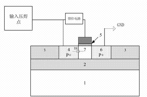
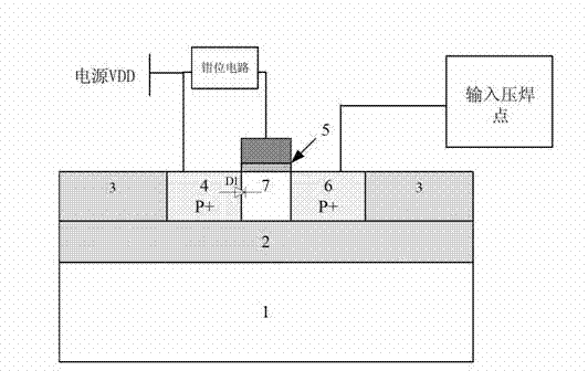
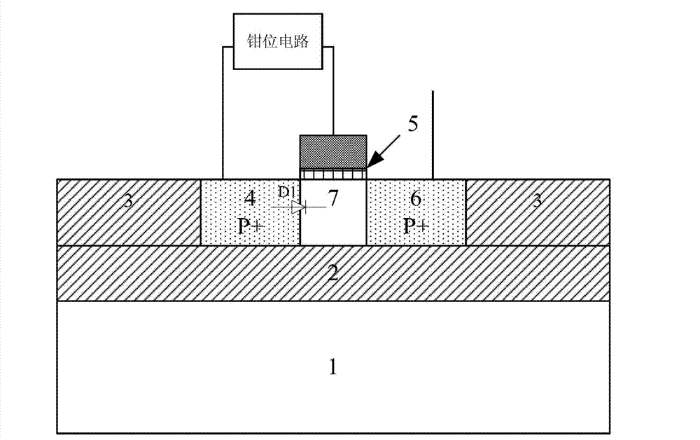
[0024] like figure 1 , as shown in 2, the present invention includes an N-type substrate PMOS tube structure, and the N-type substrate PMOS tube structure includes: gate (ploy gate) 5, P+ source diffusion region 4, P+ drain diffusion region 6, N well 7. Silicon dioxide isolation region 3, buried oxide layer (BOX) 2 and silicon substrate 1, the buried oxide layer 2 is located on the silicon substrate 1, the P+ source diffusion region 4, P+ drain diffusion region 6, The N well 7 and the silicon dioxide isolation region 3 are located on the buried oxide layer 2; the N well 7 is located between the P+ source diffusion region 4 and the P+ drain diffusion region 6, and between the P+ source diffusion region 4 and the N well 7 A parasitic diode D1 is formed, and a silicon dioxide isolation region 3 surrounds the P+ source diffusion region 4 and the P+ drain d...


PUM


Abstract

The invention relates to an ESD (Electronic Static Discharge) protection structure based on a partial depletion mode SOI (Silicon on Insulator) process. A common enhanced PMOS (P-channel Metal Oxide Semiconductor) transistor in an SOI process is used, substrate contact is not needed, a P+ / N well parasitic diode of the source end of the PMOS transistor is used for offsetting an N well; and the grid electrode of the PMOS transistor is offset by using a clamp circuit. The capacity of carrying out ESD protection is improved by using a reverse breakdown principle. The ESD protection structure has the advantages of simple structure and small occupation layout area in an SOI / CMOS integrated circuit, is convenient for use, and effectively improves the ESD tolerance level of the integrated circuit.

Description

technical field [0001] The invention relates to an ESD protection structure based on a partially depleted SOI process, belonging to the technical field of integrated circuits. Background technique [0002] SOI technology refers to the material preparation technology of forming a single crystal semiconductor silicon thin film layer with a certain thickness on the insulating layer and the process technology of manufacturing semiconductor devices on the thin film layer. This technology can achieve complete dielectric isolation. Compared with bulk silicon devices isolated by P-N junctions, it has the advantages of no latch, high speed, low power consumption, high integration, high temperature resistance, and radiation resistance. [0003] According to the thickness of SOI silicon film, SOI devices can be divided into thick film devices and thin film devices. For thick-film SOI devices, when the thickness of the SOI silicon film is greater than twice the maximum depletion width,...

Claims


Application Information

Patent Timeline
IPC IPC(8): H01L27/02
Inventor 高国平周毅罗静
Owner 58TH RES INST OF CETC
Learn More