Silicon-based InGaAs PIN photoelectric detector based on heterogeneous integration and vertical optical coupling

A photodetector and vertical coupling technology, applied in the coupling of optical waveguides, circuits, electrical components, etc., can solve problems such as the impact of bonding yield

Active Publication Date: 2012-11-14
SHANGHAI INST OF MICROSYSTEM & INFORMATION TECH CHINESE ACAD OF SCI
View PDF1 Cites 18 Cited by
  • Summary
  • Abstract
  • Description
  • Claims
  • Application Information

AI Technical Summary

Problems solved by technology

The inventors of the present invention have found through in-depth research and analysis that although the latter separates the light absorption path from the propagation path of electron-hole pairs, thus avoiding the mutual constraint between the responsivity and the bandwidth limited by the transit time, it usually requires A very thin BCB bonding layer (usually <200nm) is used to achieve efficient coupling between the waveguide and the detector, and at s...

Method used


Image

  • Silicon-based InGaAs PIN photoelectric detector based on heterogeneous integration and vertical optical coupling
  • Silicon-based InGaAs PIN photoelectric detector based on heterogeneous integration and vertical optical coupling
  • Silicon-based InGaAs PIN photoelectric detector based on heterogeneous integration and vertical optical coupling

Examples


Embodiment Construction

[0029] The device structure of the present invention will be further described below in conjunction with the accompanying drawings, which are not drawn to scale for the convenience of illustration.

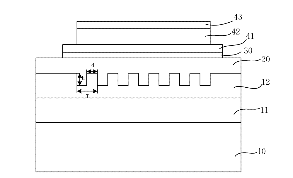
[0030] This embodiment provides a silicon-based InGaAs PIN photodetector based on heterogeneous integration and vertical optical coupling, such as figure 1 shown, including:

[0031] SOI substrate, the SOI substrate includes an underlying substrate 10, a buried oxide layer (BOX, buried oxide) 11 located on the underlying substrate 10, and a top silicon layer 12 located on the buried oxide layer 11;

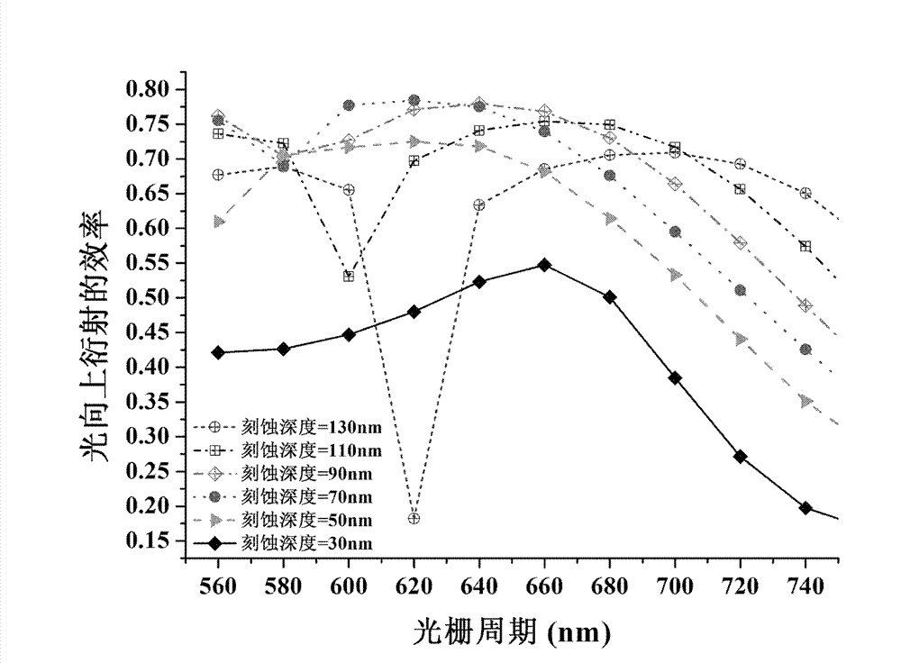
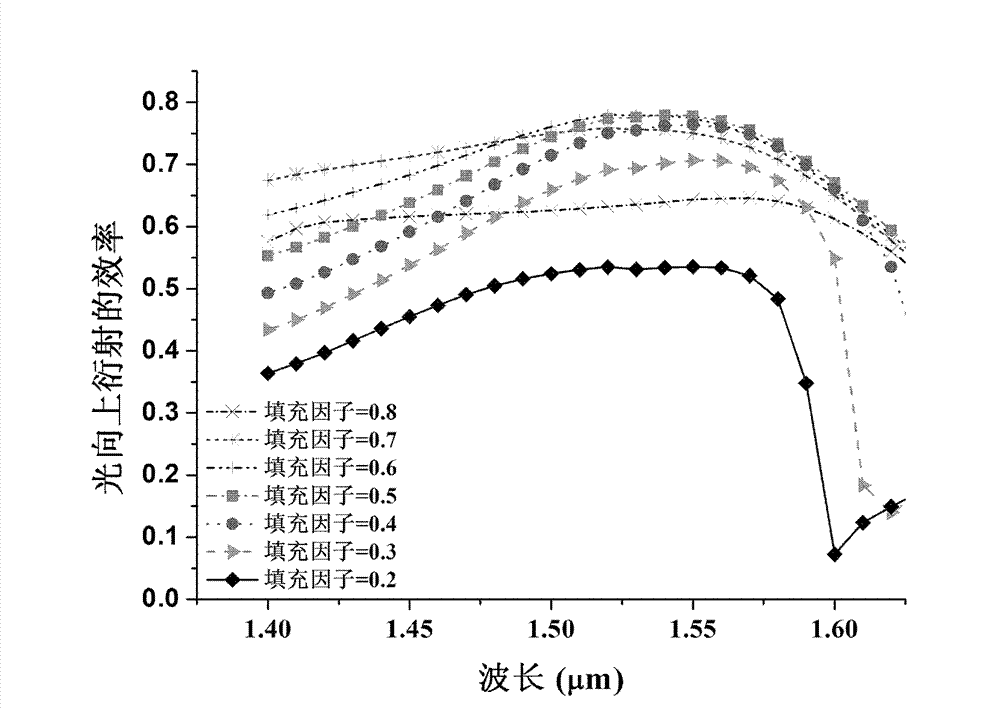
[0032] a vertical coupling grating fabricated in the top silicon 12 of the SOI substrate, the vertical coupling grating is made by etching the top silicon 12 of the SOI substrate, figure 1 where h is the etching depth, T is the grating period, and d is the grating tooth width;

[0033] a BCB bonding layer 20 covering the vertical coupling grating;

[0034] An anti-reflection layer ...


PUM

PropertyMeasurementUnit
Etching depthaaaaaaaaaa

Abstract

The invention discloses a silicon-based InGaAs PIN photoelectric detector based on heterogeneous integration and vertical optical coupling. The silicon-based InGaAs PIN photoelectric detector comprises a silicon-on-insulator (SOI) substrate, a vertical coupling grating, a benzocyclobutene (BCB) bonding layer, an anti-reflecting layer, a first conductivity type indium phosphide layer, an intrinsic InGaAs layer and a second conductivity type indium phosphide layer, wherein the vertical coupling grating is produced in top silicon of the SOI substrate, the BCB bonding layer is covered on the vertical coupling grating, the anti-reflecting layer is located above the BCB bonding layer, the first conductivity type indium phosphide layer is located above the anti-reflecting layer, the intrinsic InGaAs layer is located above the first conductivity type indium phosphide layer, the second conductivity type indium phosphide layer is located above the intrinsic InGaAs layer, the vertical coupling grating is produced by etching the top silicon of the SOI substrate, the etching depth is 70-110 nm, the grating period is 600-680 nm, and the refractive index of the anti-reflecting layer is between refractive indexes of the BCB bonding layer and the first conductivity type indium phosphide layer. According to the silicon-based InGaAs PIN photoelectric detector, by means of an adhesiveness bonding process, InP/InGaAs/InP stack material layers are adhered to the grating which is etched on the SOI substrate, so that light and the InP/InGaAs/InP layers are vertically coupled, and suitable designs and prioritization schemes are provided for specific applications of the silicon-based InGaAs PIN photoelectric detector.

Description

technical field [0001] The invention relates to a photodetector with a PIN structure, in particular to a photodetector with a PIN structure using a silicon-based InGaAs material based on heterogeneous integration and vertical optical coupling technology, and belongs to the field of semiconductor devices. Background technique [0002] Silicon photonics was proposed by Soref in the late 1980s, and has entered a period of rapid development in recent years. As a platform for optical integration, silicon has good light transmission, and due to the relatively high refractive index difference between silicon and silicon dioxide, waveguides with submicron-sized cross-sections and micron-scale bending radii can be realized, which is conducive to the realization of optical devices large-scale integration. Moreover, silicon-based optical integration technology is also compatible with CMOS technology. By applying high-quality and large-scale CMOS technology to integrate integrated circ...

Claims


Application Information

Patent Timeline
IPC IPC(8): H01L31/105H01L31/0232H01L31/0216G02B6/34
Inventor 盛振仇超甘甫烷武爱民杜骏杰陈静王曦邹世昌
Owner SHANGHAI INST OF MICROSYSTEM & INFORMATION TECH CHINESE ACAD OF SCI
Why Eureka
Try Eureka