White organic electroluminescent device and manufacturing method thereof
A luminescence and electromechanical technology, applied in semiconductor/solid-state device manufacturing, electric solid-state devices, electrical components, etc., can solve problems such as yellowish color coordinates and complex device structures, and achieve the effect of ensuring color stability
- Summary
- Abstract
- Description
- Claims
- Application Information
AI Technical Summary
Problems solved by technology
Method used
Image
Examples
Embodiment 1
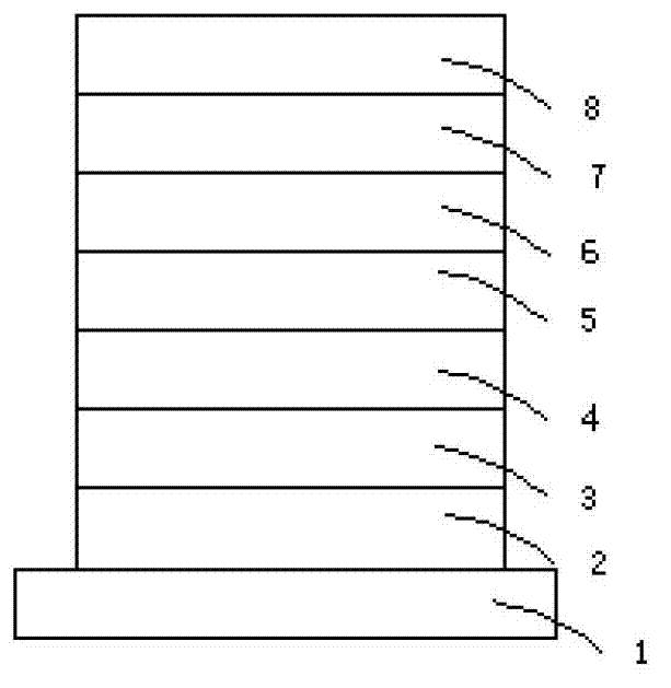
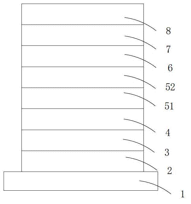
[0059] Such as figure 2 , the structure of the organic electrowhite light device in Example 1 has the following structural formula: Glass / ITO / NPB / NPB:(t-bt)2Ir(acac) / CBP / CBP:TPBi / BH:BD / Bebq2 / LiF / Al;
[0060] In Embodiment 1, the composite inner connection layer includes a bipolar connection layer 51 and a bipolar doped connection layer 52 arranged from bottom to top;
specific Embodiment approach
[0061] According to a specific implementation mode, the preparation method of the white organic electroluminescent device of the present embodiment is as follows:
[0062] The transparent conductive substrate ITO glass was ultrasonically cleaned with ethanol solution, acetone solution and deionized water, and dried with high-purity dry nitrogen after cleaning. Wherein the ITO film on the glass substrate is used as the anode conductive layer of the device, the square resistance of the ITO film is 10Ω-50Ω, and the film thickness is 100nm-200nm.
[0063] The dried ITO glass was moved into the pretreatment chamber, and the backplane was subjected to oxygen plasma treatment for 5 minutes under an environment with an oxygen partial pressure of 25Pa, and the power was 100W.
[0064] Place the above-mentioned cleaned and pretreated ITO glass in a vacuum chamber, and evacuate to 5×10 -4 Pa, and then vapor-deposit a layer of hole-transporting material NPB on the above-mentioned ITO fil...
Embodiment 2
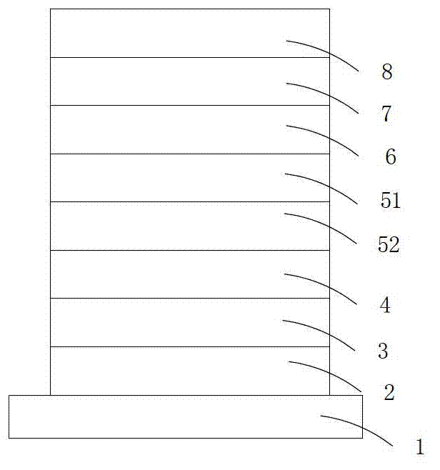
[0084] Such as image 3 As shown, the structure of the organic electrowhite light device in Example 2 has the following structural formula: Glass / ITO / NPB / NPB:(t-bt)2Ir(acac) / CBP:TPBi / CBP / BH:BD / Bebq2 / LiF / Al;
[0085] In Embodiment 2, the composite inner connection layer includes a bipolar doped connection layer 52 and a bipolar connection layer 51 arranged from bottom to top;
[0086] The structure of the composite connection layer in Embodiment 2 is a double-layer structure, and the bipolar doped connection layer 52 is composed of a bipolar transmission material CBP doped with a unipolar transmission material TPBi, and is close to the first yellow light layer. side; the bipolar connection layer 51 is an auxiliary transition layer composed of CBP, which is close to the blue light side.
[0087] The preparation method of the device of embodiment 2 is similar to that of embodiment 1, the difference is that: the bipolar connection layer 51 and the bipolar doped connection layer...
PUM
| Property | Measurement | Unit |
|---|---|---|
| Sheet resistance | aaaaa | aaaaa |
| Film thickness | aaaaa | aaaaa |
| Thickness | aaaaa | aaaaa |
Abstract
Description
Claims
Application Information


