Microfluidic surface-enhanced Raman scattering detector and its preparation method and use

A surface-enhanced Raman and microfluidic technology, used in Raman scattering, material excitation analysis, etc., can solve the problem that the distribution cannot achieve good uniformity, the time consuming often takes several hours or even longer, and the amount of reagents is large. And other issues

Active Publication Date: 2012-11-21
PEKING UNIV
View PDF10 Cites 17 Cited by
  • Summary
  • Abstract
  • Description
  • Claims
  • Application Information

AI Technical Summary

Problems solved by technology

When the immersion-evaporation method is used, a layer of analyte molecules can be evenly adsorbed on the nano-rough surface or nano-structure of the open active substrate, but this method requires a large amount of reagents, and the soaking time often takes several hours. hours or more
When the titration-evaporation method is used to distribute the analyte, the required reagent dose only needs to cover the entire surface of the active substrate in the horizontal direction, but its height may reach the order of millimeters, so the reagent consumption is still relatively large; and ...

Method used


Image

  • Microfluidic surface-enhanced Raman scattering detector and its preparation method and use
  • Microfluidic surface-enhanced Raman scattering detector and its preparation method and use
  • Microfluidic surface-enhanced Raman scattering detector and its preparation method and use

Examples


Embodiment 1

[0066] Preparation of an active substrate containing several nano-hole structures covered with a metal layer:

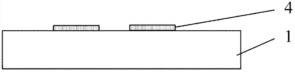
[0067] 1') Spin-coat RZJ-304 positive photoresist with a thickness of 2 μm on the surface of the silicon substrate 1, pre-bake it in a 98°C oven for 15 minutes, use a wavelength of 365nm, and an intensity of 5.4mW / cm 2 The ultraviolet light is exposed through the mask plate 1 for 10s, and after developing for 30s in the developer of RZJ-304 positive photoresist, a nanochannel composed of multiple small photoresist patterns and their gaps is formed. The gap width 100µm, such as figure 1 shown;

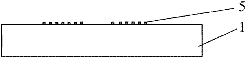
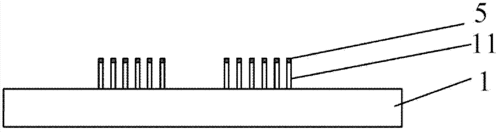
[0068] 2') Put the silicon substrate 1 obtained in step 1') with nanochannels composed of multiple small photoresist patterns and gaps together into an oxygen plasma bombardment chamber with a power of 250W and an oxygen flow rate of 30sccm , bombard the photoresist for 10 minutes, and generate point-like nanomaterial structures uniformly distributed on the silicon substrate...

Embodiment 2

[0078] Preparation of an active substrate containing several nano-hole structures covered with a metal layer:

[0079] 1') Spin-coat RZJ-304 positive photoresist with a thickness of 2 μm on the surface of the silicon substrate 1, pre-bake it in a 98°C oven for 15 minutes, use a wavelength of 365nm, and an intensity of 5.4mW / cm 2 The ultraviolet light is exposed through the mask plate 1 for 10s, and after developing for 30s in the developer of RZJ-304 positive photoresist, a nanochannel composed of multiple small photoresist patterns and their gaps is formed. The gap width 100µm, such as figure 1 shown;

[0080] 2') Put the silicon substrate 1 obtained in step 1') with nanochannels composed of multiple small photoresist patterns and gaps together into an oxygen plasma bombardment chamber with a power of 250W and an oxygen flow rate of 30sccm , bombard the photoresist for 10 minutes, and generate point-like nanomaterial structures uniformly distributed on the silicon substrate...

Embodiment 3

[0091] Preparation of an active substrate containing several nano-hole structures covered with a metal layer:

[0092] 1') Spin-coat RZJ-304 positive photoresist with a thickness of 2 μm on the surface of the silicon substrate 1, pre-bake it in a 98°C oven for 15 minutes, use a wavelength of 365nm, and an intensity of 5.4mW / cm 2 The ultraviolet light is exposed through the mask plate 1 for 10s, and after developing for 30s in the developer of RZJ-304 positive photoresist, a nanochannel composed of multiple small photoresist patterns and their gaps is formed. The gap width 100µm, such as figure 1 shown;

[0093] 2') Put the silicon substrate 1 obtained in step 1') with nanochannels composed of multiple small photoresist patterns and gaps together into an oxygen plasma bombardment chamber with a power of 250W and an oxygen flow rate of 30sccm , bombard the photoresist for 10 minutes, and generate point-like nanomaterial structures uniformly distributed on the silicon substrate...


PUM

PropertyMeasurementUnit
Thicknessaaaaaaaaaa
Diameteraaaaaaaaaa
Heightaaaaaaaaaa

Abstract

The invention discloses a microfluidic surface-enhanced Raman scattering detector and its preparation method and use. The microfluidic surface-enhanced Raman scattering detector comprises an active base and a microfluidic channel-containing structure layer. A microfluidic channel chamber is formed between the active base and the microfluidic channel-containing structure layer. The active base corresponding to the microfluidic channel chamber is provided with multiple nanoscale concave structures. The microfluidic channel-containing structure layer corresponding to the microfluidic channel chamber is provided with at least one pair of a liquid inlet and a liquid outlet communicated with the microfluidic channel chamber. A metal layer is coated on nanoscale concave structure surfaces and an active base surface located in the microfluidic channel chamber. The microfluidic surface-enhanced Raman scattering detector having a double-layer polydimethylsiloxane structure has a high yield, a low cost, good detection consistency and no noise interference and can realize real-time monitoring. The microfluidic surface-enhanced Raman scattering detector can be used for detection of an analyte in gas, colloid and liquid environments.

Description

technical field [0001] The invention relates to a microfluidic surface-enhanced Raman scattering detection device, in particular to a microfluidic surface-enhanced Raman scattering detection device and its preparation method and application. Background technique [0002] Raman scattering detection is a method of material structure analysis that does not require labeling of the sample to be detected, and has the characteristics of non-destructive and contact-free. With the development of laser technology and weak signal detection and reception technology, as a means to realize the molecular level detection of material structure, Raman scattering detection is expected to be practical and widely used in the fields of biological detection, disease diagnosis, environmental monitoring, chemical analysis and so on. Applications. However, due to the small Raman scattering cross-section and the low analytical sensitivity of Raman scattering detection, it is difficult to obtain Raman...

Claims


Application Information

Patent Timeline
IPC IPC(8): G01N21/65
Inventor 吴文刚毛海央吕芃芃
Owner PEKING UNIV
Why Eureka
Try Eureka