Manufacturing method for GaN (gallium nitride) based LED (light emitting diode) chip

A technology of LED chip and manufacturing method, applied in semiconductor/solid-state device manufacturing, semiconductor device, electrical components and other directions, can solve problems such as low contact resistance

Inactive Publication Date: 2012-11-21
ANHUI SANAN OPTOELECTRONICS CO LTD
View PDF2 Cites 9 Cited by
  • Summary
  • Abstract
  • Description
  • Claims
  • Application Information

AI Technical Summary

Problems solved by technology

ITO used as the contact material of n-type GaN can obtain transparent low-resistance ohmic contact, but the direct use of ITO as the

Method used


Image

  • Manufacturing method for GaN (gallium nitride) based LED (light emitting diode) chip
  • Manufacturing method for GaN (gallium nitride) based LED (light emitting diode) chip
  • Manufacturing method for GaN (gallium nitride) based LED (light emitting diode) chip

Examples


Embodiment 1

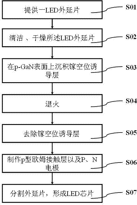
[0036] The specific implementation steps of a method for manufacturing a GaN-based LED chip are as follows:

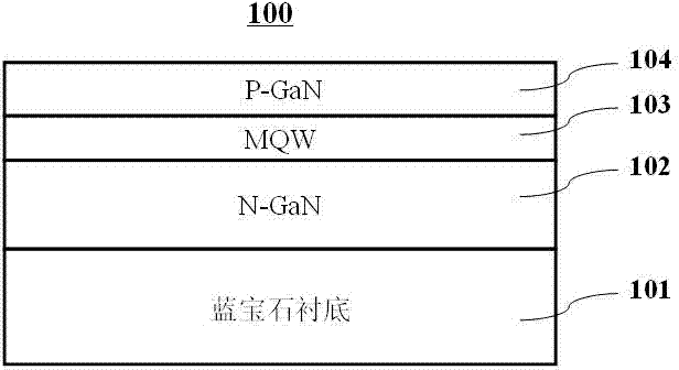
[0037] Such as figure 2 As shown, a GaN epitaxial wafer 100 (hereinafter referred to as a sample) to be fabricated is provided, including a growth substrate 101, an n-GaN layer 102, a light emitting layer 103, and a p-GaN layer 104, and the sample is cleaned with HCl, BOE, and aqua regia. and dry it.

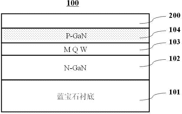
[0038] Such as image 3 As shown, a Ni / Au metal thin film is deposited on the surface of the p-GaN sample as the gallium vacancy inducing layer 200 by ion sputtering or vacuum electron beam evaporation coating equipment, the thickness of Ni is 3nm, and the thickness of Au is 10nm.

[0039] Such as Figure 4 As shown, the sample was annealed in a high-temperature furnace tube, the atmosphere was nitrogen, and the temperature was 500°C.

[0040] Such as Figure 5 As shown, the samples were successively placed in KI and dilute nitric acid solution to remove Ni / Au on t...

Embodiment 2

[0045] The difference between this embodiment and the first embodiment is that this embodiment is used to form a vertical LED chip, and the gallium holes on the surface of the activated p-GaN are processed in the same way as the first embodiment, the difference lies in the subsequent chip process, After removing the Ni / Au gallium vacancy inducing layer 200 on the sample surface, the specific steps include:

[0046] First, a Ni / Ag / Pt highly reflective p-type ohmic contact layer is fabricated on the p-GaN surface;

[0047] In the next step, a Ti / Pt / Au bonding metal layer is deposited on the entire sample surface to form a mirror metal bonding layer;

[0048] In the next step, a Si sheet is provided as a supporting substrate 600, a bonding metal layer Ti / Pt / Au is deposited on its surface, and the sample is bonded to the Si sheet using vacuum bonding equipment;

[0049] In the next step, the growth substrate of the sample is peeled off using laser lift-off equipment to expose the...


PUM

PropertyMeasurementUnit
Thicknessaaaaaaaaaa

Abstract

The invention discloses a manufacturing method for a GaN (gallium nitride) based LED (light emitting diode) with a low series resistance and a good p type ohmic contact. The manufacturing method comprises the following steps: 1) providing a GaN based LED epitaxial wafer; 2) cleaning and drying the GaN based LED epitaxial wafer; 3) depositing a gallium vacancy induction layer on a p-GaN surface of the epitaxial wafer; 4) annealing the GaN based LED epitaxial wafer; 5) removing the gallium vacancy induction layer from the surface of the GaN based LED epitaxial wafer; 6) manufacturing a p type ohmic contact layer and electrodes P and N on the treated GaN based LED epitaxial wafer; and 7) dividing the GaN based LED epitaxial wafer into LED chip particles.

Description

technical field [0001] The invention relates to a method for manufacturing a semiconductor light-emitting element, more specifically a method for manufacturing a GaN-based LED chip with low series resistance and good p-type ohmic contact. Background technique [0002] Light-emitting diodes of solid-state light-emitting devices have low energy consumption, long life, good stability, small size, fast response speed, and stable light-emitting wavelength and other good optoelectronic properties, and are widely used in lighting, home appliances, display screens, and indicator lights. This type of light-emitting device has made considerable progress in terms of light efficiency and service life, and is expected to become the mainstream of a new generation of lighting and light-emitting devices. [0003] Although GaN-based devices have made considerable progress in recent years, the development of GaN-based high-temperature and high-power devices has been limited due to the difficu...

Claims


Application Information

Patent Timeline
IPC IPC(8): H01L21/324H01L33/00
Inventor 陈顺平潘群峰曾晓强黄少华
Owner ANHUI SANAN OPTOELECTRONICS CO LTD
Why Eureka
Try Eureka