

Enhanced A1N/GaN high-electron mobility transistor and fabrication method thereof
A high electron mobility, transistor technology, applied in semiconductor/solid-state device manufacturing, circuits, electrical components, etc., can solve problems such as high annealing temperature, lattice damage, poor thermal stability, etc., achieve precise control of device threshold, reduce pass State resistance, high reliability effect
- Summary
- Abstract
- Description
- Claims
- Application Information
AI Technical Summary
Problems solved by technology
Method used
Image

Examples
Embodiment Construction
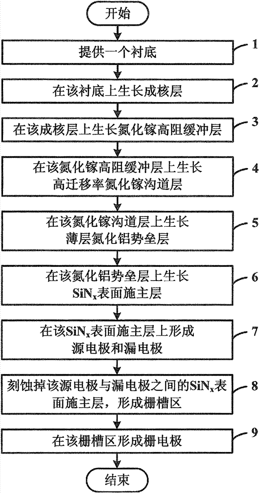
[0039] In order to make the object, technical solution and advantages of the present invention clearer, the present invention will be described in further detail below in conjunction with specific embodiments and with reference to the accompanying drawings. Of course, they are only examples and are not intended to limit the invention.
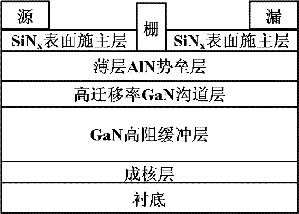
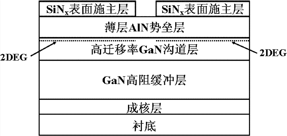
[0040] The invention utilizes epitaxial structure and material energy band control to fabricate ultra-thin barrier AlN / GaN heterojunction, so that two-dimensional electron gas (2DEG) cannot be formed at the heterojunction, and is used to realize the pinch-off region of the channel; another On the one hand, depositing SiN on the ultra-thin barrier AlN / GaN heterojunction x surface donor layer, which facilitates the SiN x A large number of positive charge donors are generated at the / AlN interface, which reduces the barrier height at the AlN surface, thereby forming a 2DEG channel at the AlN / GaN interface, and the AlN / GaN HEMT has extremely stron...
PUM
| Property | Measurement | Unit |
|---|---|---|
| Thickness | aaaaa | aaaaa |
Abstract
Description
Claims
Application Information