Light-emitting element, light-source apparatus and projection-type display apparatus
A technology of light-emitting components and optical components, applied in electroluminescent light sources, light sources, electric light sources, etc., can solve problems such as limitations, achieve high directivity, improve brightness and directivity, and high brightness effects
- Summary
- Abstract
- Description
- Claims
- Application Information
AI Technical Summary
Problems solved by technology
Method used
Image

Examples
no. 1 example )
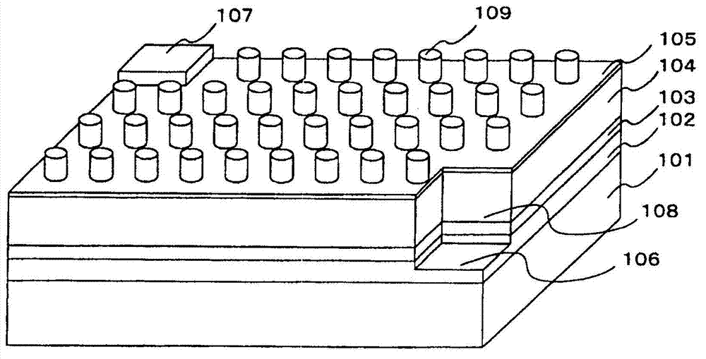
[0057] Figure 3A is a schematic diagram schematically showing the configuration of the light emitting element according to the first embodiment of the present invention. Figure 3B is a plan view schematically showing the light emitting element according to the first embodiment of the present invention. Because the individual layers of the light-emitting element are very thin and their thicknesses vary greatly, it is difficult to draw precise proportions of the individual layers. Therefore, in the drawings, the respective layers are not drawn in actual scale but are schematically shown.
[0058] Such as Figure 3A As shown, the light-emitting element 1 according to the first embodiment has a light source layer 4 and a direction control layer 5 which is stacked on the light source layer 4 and performed as an optical element layer into which light from the light source layer 4 enters. Work.
[0059] Light source layer 4 has substrate 10 and a pair of hole transport layer 11...
no. 2 example )
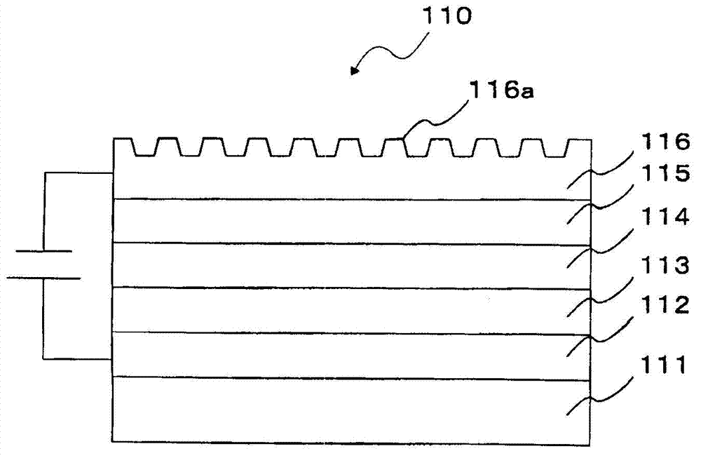
[0102] Figure 4A is a perspective view schematically showing a light emitting element according to a second embodiment of the present invention. Figure 4B is a plan view schematically showing the light emitting element according to the second embodiment.
[0103] Such as Figure 4A and Figure 4B As shown, the optical element 2 according to the second embodiment has a light source layer 24 and a direction control layer 5 which is stacked on the light source layer 24 and into which light from the light source layer 24 enters. Since the directional control layer 5 of the optical element 2 according to the second embodiment is the same as that of the first embodiment, description of the directional control layer 5 will be omitted. Light source layer 24 of optical element 2 according to the second embodiment differs from light source layer 4 according to the first embodiment only in that active layer 12 is formed between hole transport layer 11 and electron transport layer 13...
no. 3 example )
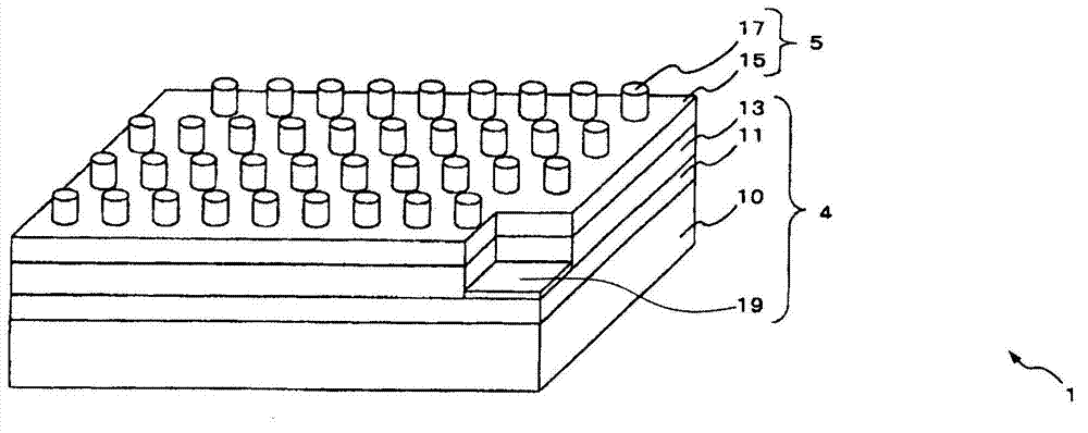
[0112] Figure 6A is a perspective view schematically showing a light emitting element according to a third embodiment of the present invention. Figure 6B is a plan view schematically showing the light emitting element according to the third embodiment.
[0113] Such as Figure 6A and Figure 6B As shown, the light emitting element 3 according to the third embodiment has a light source layer 34 and a direction control layer 5 which is stacked on the light source layer 34 and into which light from the light source layer 34 enters. Since the directional control layer 5 of the optical element 3 according to the third embodiment is the same as that of the first embodiment, description of the directional control layer 5 will be omitted. Light source layer 34 of optical element 3 according to the third embodiment differs from light source layer 24 according to the second embodiment only in that anode layer 29 (which serves as an anode) is completely formed between substrate 10 a...
PUM
 Abstract
Description
Claims
Application Information
 - R&D
- Intellectual Property
- Life Sciences
- Materials
- Tech Scout
- Unparalleled Data Quality
- Higher Quality Content
- 60% Fewer Hallucinations
Browse by: Latest US Patents, China's latest patents, Technical Efficacy Thesaurus, Application Domain, Technology Topic, Popular Technical Reports.
© 2025 PatSnap. All rights reserved.Legal|Privacy policy|Modern Slavery Act Transparency Statement|Sitemap|About US| Contact US: help@patsnap.com