A kind of preparation method of sige-hbt transistor based on soi

A technology of transistors and base regions, applied in the manufacture of semiconductor/solid-state devices, semiconductor devices, electrical components, etc., can solve the problem of small vertical width of the collector region, reduction of the maximum cut-off frequency Ft parameter, increase of SiGe-HBT device collector resistance, etc. problems, to achieve the effect of avoiding the increase of doping concentration, easy to realize, and simple preparation process

Inactive Publication Date: 2014-10-08
SHANGHAI INST OF MICROSYSTEM & INFORMATION TECH CHINESE ACAD OF SCI
View PDF4 Cites 0 Cited by
  • Summary
  • Abstract
  • Description
  • Claims
  • Application Information

AI Technical Summary

Problems solved by technology

But for the thin-film SOI process, because the top silicon film is very thin (less than or equal to 0.15um), the vertical width of the collector region is small, and the extra base region formed by the downward extension of the outer base implantation will cause the collector resistance of the SiGe-HBT device to increase significantly. increase and the highest cut-off frequency Ft parameter is significantly lower

Method used


Image

  • A kind of preparation method of sige-hbt transistor based on soi
  • A kind of preparation method of sige-hbt transistor based on soi
  • A kind of preparation method of sige-hbt transistor based on soi

Examples


Embodiment 1

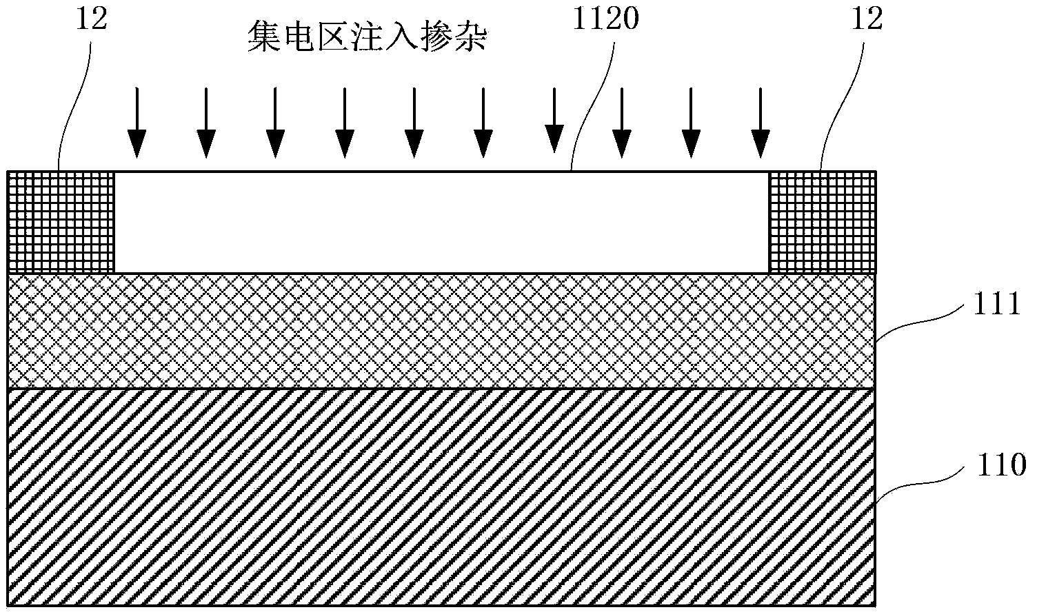
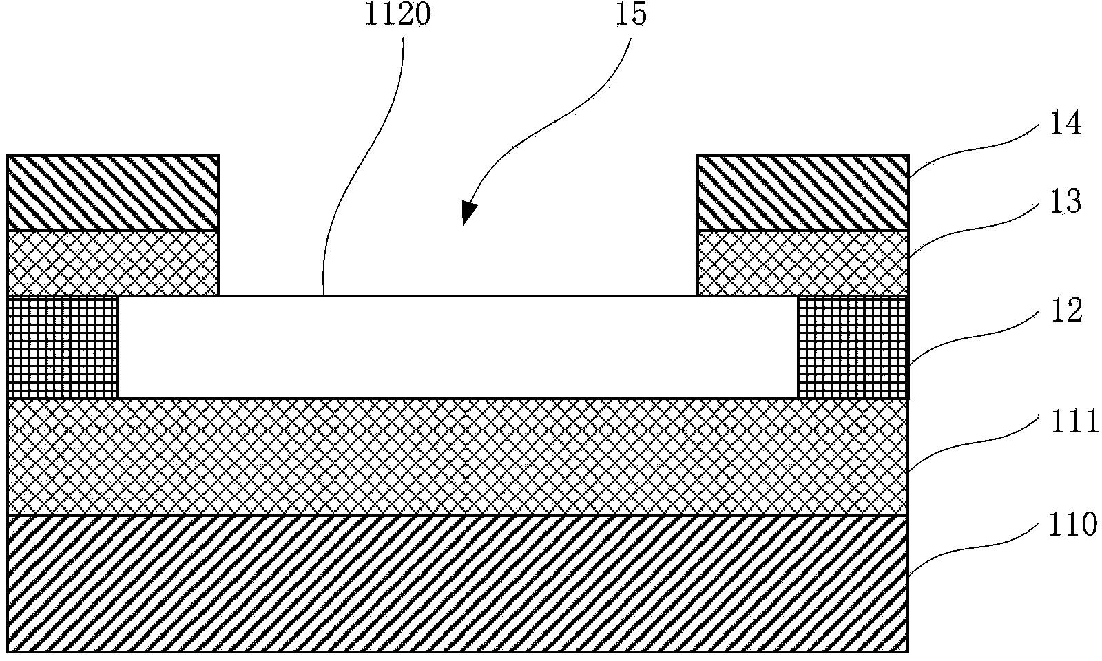
[0048] Control attached Figure 1a to Figure 1k , the present invention provides a method for preparing an SOI-based vertical SiGe-HBT, comprising the following steps:

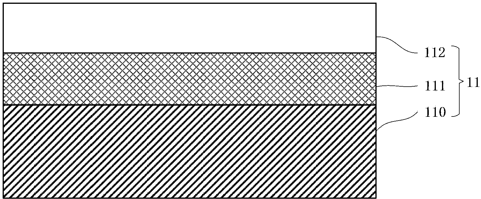
[0049] Step 1: If Figure 1a to Figure 1b As shown, an SOI substrate 11 is provided, including a back substrate silicon 110, a buried layer silicon oxide 111 and a top layer silicon 112, wherein the SOI substrate 11 is a conventional SOI starting wafer, and the thickness of the buried layer silicon oxide 111 is 100nm-200nm, the thickness of the top layer silicon 112 is 50nm-150nm. In this embodiment, the thickness of the buried layer silicon oxide 111 is temporarily selected as 150 nm, and the thickness of the top layer silicon 112 is temporarily selected as 100 nm, but it is not limited thereto. In other embodiments, other thicknesses can also be used, such as the buried layer The thickness of the silicon oxide 111 may be 100nm, 120nm, 180nm, or 200nm, etc., and the thickness of the top layer silicon 112 may ...


PUM


Abstract

Provided is a method of manufacturing an SOI-based silicon-germanium heterojunction bipolar transistor (SiGe-HBT). In the method, the impurity injected in an outer base region (161) is changed from boron to boron fluoride, and the injection energy and amount are defined in specific ranges, thereby effectively solving the problems of significantly increased collector resistance and an apparently reduced maximum cut-off frequency Ft parameter for SiGe-HBT devices on a thin-film SOI. Also, compared with other methods of increasing an injection amount and a doping concentration in a collector region, the method avoids lowered voltage endurance of devices because of an increased doping concentration in a collector region. In addition, the manufacturing process is simple and is easy to implement.

Description

technical field [0001] The invention belongs to the field of solid electronics and microelectronics, and relates to a method for preparing a SiGe bipolar transistor, in particular to a method for preparing an SOI-based SiGe bipolar transistor (SiGe-HBT). Background technique [0002] Due to the demand for high-performance, low-noise and low-cost RF components in high-frequency bands for modern communications, traditional Si material devices cannot meet new requirements such as performance specifications and output power. The silicon-germanium heterojunction bipolar transistor (SiGe-HBT) formed by introducing Ge into the Si material as the base of the bipolar transistor is favored by the market due to its low cost and high performance potential. Under the same conditions, SiGe devices have higher frequency, faster speed, lower noise, and higher current gain than Si devices, and are suitable for high-frequency applications. The SiGeHBT process is a silicon-based technology, a...

Claims


Application Information

Patent Timeline
Patent Type & Authority Patents(China)
IPC IPC(8): H01L21/331H01L21/266H01L29/737
CPCH01L29/7378H01L29/66242
Inventor 柴展陈静罗杰馨伍青青王曦
Owner SHANGHAI INST OF MICROSYSTEM & INFORMATION TECH CHINESE ACAD OF SCI
Why Eureka
Try Eureka