Thin film transistor and manufacturing method thereof as well as array substrate and display device

A technology of a thin film transistor and a manufacturing method, applied in the fields of an array substrate, a thin film transistor and a manufacturing method thereof, and a display device, can solve the problems of large device size, low mobility, poor stability, etc., and achieves reduction of metal impurity content and low process temperature. , the effect of inducing metal content control

Inactive Publication Date: 2012-12-26
BOE TECH GRP CO LTD
View PDF2 Cites 4 Cited by
  • Summary
  • Abstract
  • Description
  • Claims
  • Application Information

AI Technical Summary

Problems solved by technology

However, due to its low mobility, large device size, and poor stability, it is difficult to apply to high-resolution TFT-LCD and current-mode driven TFT-OLED.

Method used


Image

  • Thin film transistor and manufacturing method thereof as well as array substrate and display device
  • Thin film transistor and manufacturing method thereof as well as array substrate and display device
  • Thin film transistor and manufacturing method thereof as well as array substrate and display device

Examples


Embodiment Construction

[0036] The following will clearly and completely describe the technical solutions in the embodiments of the present invention with reference to the accompanying drawings in the embodiments of the present invention. Obviously, the described embodiments are only some, not all, embodiments of the present invention. Based on the embodiments of the present invention, all other embodiments obtained by persons of ordinary skill in the art without making creative efforts belong to the protection scope of the present invention.

[0037] It should be noted that the terms "upper" and "lower" in the present invention are only used to describe the present invention with reference to the accompanying drawings, and are not used as limiting terms.

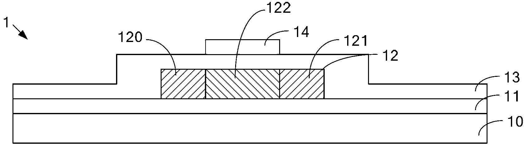
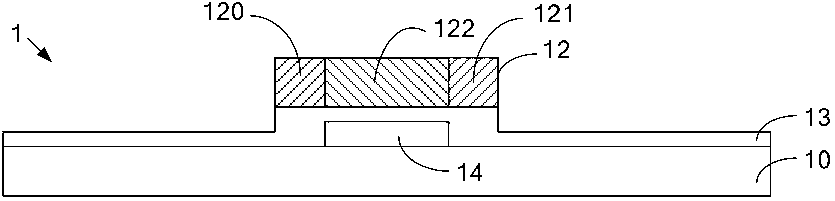
[0038] The thin film transistor provided by the embodiment of the present invention includes a substrate, a gate and a gate insulating layer disposed on the substrate, and is characterized in that it also includes:

[0039] The active layer arrang...


PUM


Abstract

The embodiment of the invention provides a thin film transistor and a manufacturing method thereof as well as an array substrate and a display device, and relates to the field of display technologies, and a thin film transistor with low impurity content can be prepared in low temperature. The thin film transistor comprises a substrate and an active layer arranged on the substrate, wherein the active layer comprises a source electrode, a drain electrode and a channel region; the active layer is formed in the way that after inductive metal is deposited on an amorphous silicon layer on the substrate through ALD (Atomic Layer Deposition), the amorphous silicon layer on which the inductive metal is deposited is subject to heat treatment to enable the amorphous silicon layer to be subject to metal-induced crystallization and metal-induced transverse crystallization; and the active layer provides the source electrode, the drain electrode and the channel region.

Description

technical field [0001] The invention relates to the field of display technology, in particular to a thin film transistor and a manufacturing method thereof, an array substrate, and a display device. Background technique [0002] With the continuous advancement of technology, users' demand for liquid crystal display equipment is increasing, and TFT-LCD (Thin Film Transistor-Liquid Crystal Display, Thin Film Field Effect Transistor Liquid Crystal Display) has also become the mainstream display used in mobile phones, tablet computers and other products . In addition, with the popularization of display devices, users' requirements for high color quality, high contrast, high viewing angle, high response speed and low power consumption are becoming more and more common. OLED (Organic Light-Emitting Diode, thin film field effect transistor organic Light-emitting diode) displays have also begun to gradually enter the user's field of vision. [0003] At present, amorphous silicon t...

Claims


Application Information

Patent Timeline
Patent Type & Authority Applications(China)
IPC IPC(8): H01L29/786H01L21/20H01L21/336
CPCH01L29/78669H01L29/66765H01L29/66757
Inventor 刘政龙春平金馝奭
Owner BOE TECH GRP CO LTD
Why Eureka
Try Eureka