Black silicon structure and manufacturing method thereof

A technology of black silicon and silicon substrate, which is applied in the field of black silicon structure and its manufacturing, can solve the problems of increased transmission and limited absorption, and achieves the effects of good absorption performance, low cost, and low noise current

Inactive Publication Date: 2012-12-26
UNIV OF ELECTRONIC SCI & TECH OF CHINA
View PDF2 Cites 16 Cited by
  • Summary
  • Abstract
  • Description
  • Claims
  • Application Information

AI Technical Summary

Problems solved by technology

But at wavelengths beyond 1100nm, if no absorption level is introduced in the silicon forbidden band, the reduced reflection only le

Method used


Image

  • Black silicon structure and manufacturing method thereof
  • Black silicon structure and manufacturing method thereof
  • Black silicon structure and manufacturing method thereof

Examples


Embodiment Construction

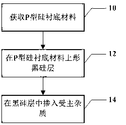
[0025] Such as figure 1 As shown, in one embodiment of the present invention, a method for manufacturing a black silicon structure includes step 10 , step 12 and step 14 .

[0026] Step 10: Obtain a P-type silicon substrate.

[0027] In the embodiment of the present invention, the substrate material is obtained first, and the black silicon result of the present invention is made based on the substrate material. In one embodiment, the substrate material may be P-type silicon. Wherein, the P-type silicon is a hole-conducting silicon material, for example, a silicon material doped with boron. Of course, it can also be P-type silicon doped with other elements.

[0028] Step 12: forming a black silicon layer on the P-type silicon substrate.

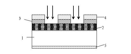
[0029] After obtaining the P-type silicon substrate, based on the P-type silicon substrate, by processing a surface of the P-type silicon substrate, at least a certain thickness of material on the surface is transformed into a black silico...


PUM


Abstract

The embodiment of the invention discloses a manufacturing method of a black silicon structure. The method comprises the following steps: a P-type silicon substrate is acquired; a black silicon layer is formed on the P-type silicon substrate; and an acceptor impurity is doped in the black silicon layer to form a doped black silicon layer. In the embodiment of the invention, the manufactured black silicon structure has favorable absorbability to both visible light and near-infrared light, and is low in noise current, high in signal-to-noise ratio, simple in structure and lower in cost.

Description

[0001] technical field [0002] The invention relates to the technical field of photosensitive materials, in particular to a black silicon structure and a manufacturing method thereof. Background technique [0003] Crystalline silicon is widely used in the semiconductor industry due to its advantages of easy purification, easy doping, and high temperature resistance, but it also has many defects, such as the high reflection of visible-infrared light on the surface of crystalline silicon, and because of Large, crystalline silicon cannot absorb light waves with a wavelength greater than 1100nm. When the wavelength of incident light is greater than 1100nm, the absorption rate and responsivity of silicon detectors to light will be greatly reduced. Other materials such as germanium and gallium indium arsenide must be used to detect these bands. The disadvantages of these materials, such as high price, poor thermodynamic properties and crystal quality, and incompatibility with...

Claims


Application Information

Patent Timeline
IPC IPC(8): H01L31/18H01L31/028
CPCY02P70/50
Inventor 李世彬张鹏吴志明蒋亚东
Owner UNIV OF ELECTRONIC SCI & TECH OF CHINA
Why Eureka
Try Eureka