Epitaxial substrate and method for producing epitaxial substrate
一种外延基板、制造方法的技术,应用在半导体/固态器件制造、半导体器件、电气元件等方向,能够解决电子迁移率低、漏电流或耐压降低、产生裂纹等问题,达到抑制应变能量的积累、弯曲小、良好结晶质量的效果
- Summary
- Abstract
- Description
- Claims
- Application Information
AI Technical Summary
Problems solved by technology
Method used
Image

Examples
Embodiment
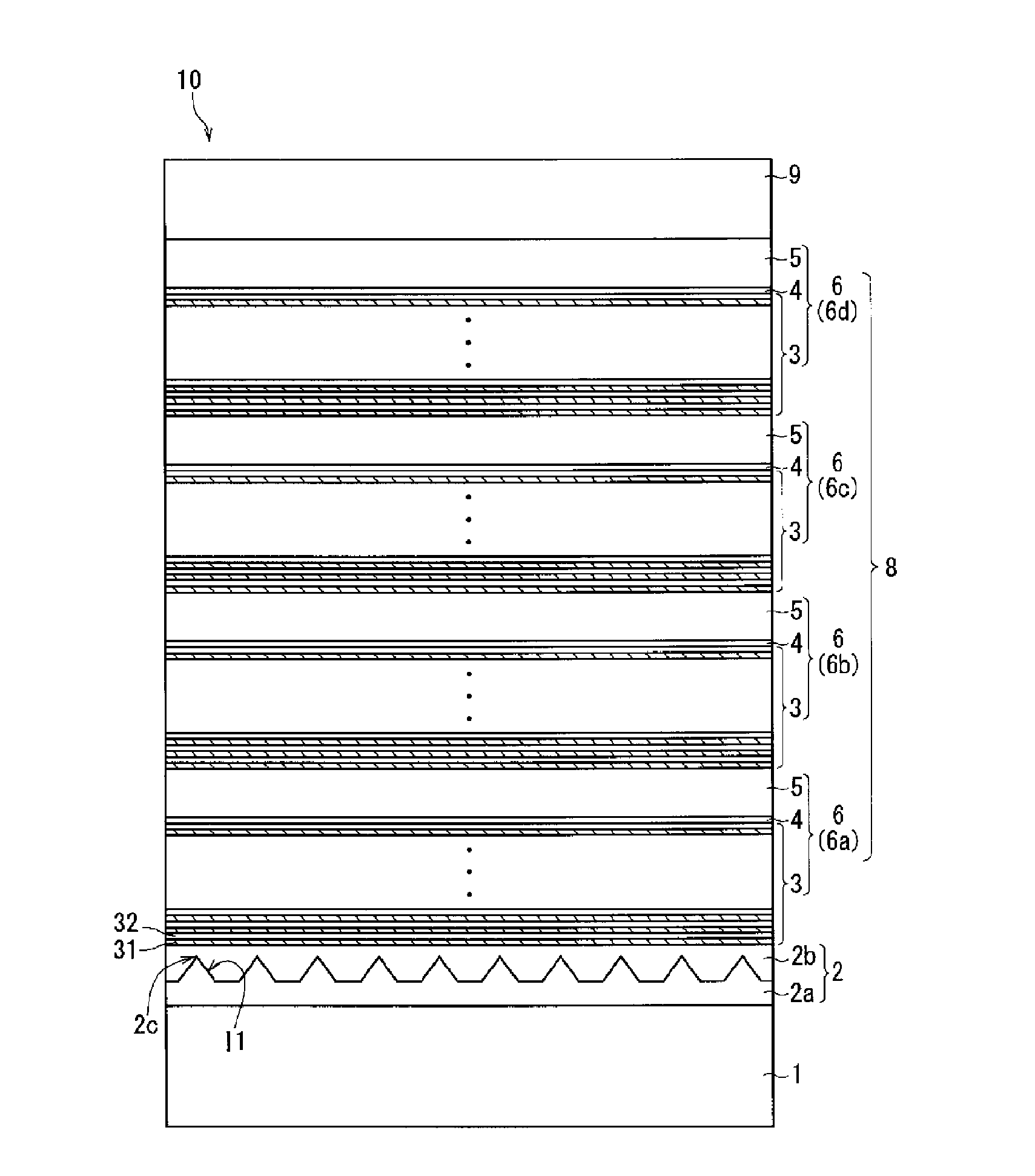
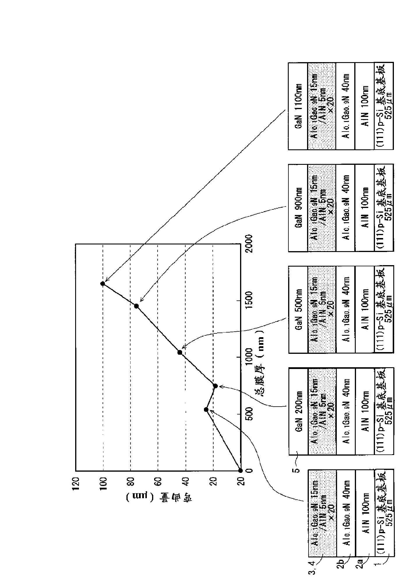
[0126] As examples, various types of epitaxial substrates 10 having different layer structures of buffer layers 8 were produced. Table 1 shows the basic structure of the epitaxial substrate 10 of the example, specifically, the formation material and film thickness of each layer.
[0127] [Table 1]
[0128]
[0129]
[0130] As shown in Table 1, in this embodiment, for all the epitaxial substrates 10, the base substrate 1, the base layer 2 (the first base layer 2a and the second base layer 2b), and the functional layer 9 are made of the same material and film thickness. form. In addition, the functional layer 9 has a two-layer structure of a channel layer and a barrier layer.
[0131] On the other hand, both the first unit layer 31 and the terminal layer 4 are formed of AlN. In Table 1, the film thickness of the first unit layer 31 is represented by a variable A (nm), and the film thickness of the terminal layer 4 is represented by a variable C (nm). Similarly, the fi...
PUM
 Abstract
Description
Claims
Application Information
 - R&D
- Intellectual Property
- Life Sciences
- Materials
- Tech Scout
- Unparalleled Data Quality
- Higher Quality Content
- 60% Fewer Hallucinations
Browse by: Latest US Patents, China's latest patents, Technical Efficacy Thesaurus, Application Domain, Technology Topic, Popular Technical Reports.
© 2025 PatSnap. All rights reserved.Legal|Privacy policy|Modern Slavery Act Transparency Statement|Sitemap|About US| Contact US: help@patsnap.com