Process for manufacturing emitter of solar cell

A solar cell and manufacturing process technology, applied in sustainable manufacturing/processing, circuits, electrical components, etc., to improve conversion efficiency, reduce production costs, and be simple and easy to operate

Inactive Publication Date: 2013-01-16
TIANWEI NEW ENERGY HLDG
View PDF8 Cites 7 Cited by
  • Summary
  • Abstract
  • Description
  • Claims
  • Application Information

AI Technical Summary

Problems solved by technology

For each pentavalent element atom, although it releases a free electron and becomes a positive ion with an electronic charge, it is bound in the lattice and cannot conduct electricity like a carrier

Method used


Image

  • Process for manufacturing emitter of solar cell

Examples


Embodiment 1

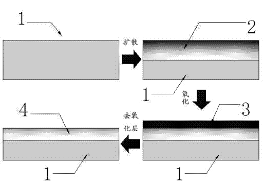
[0043] Such as figure 1 shown.

[0044] Step A: using a diffusion process to form a PN junction on the surface of the substrate silicon wafer 1 to form a surface impurity distribution layer 2;

[0045] Step B: performing oxidation treatment on the surface impurity distribution layer 2 in step A, and rapidly growing a uniformly distributed oxide layer 3 on the surface of the surface impurity distribution layer 2;

[0046] Step C: removing the oxide layer 3 in step B.

Embodiment 2

[0048] Such as figure 1 shown.

[0049] Step A: using a diffusion process to form a PN junction on the surface of the substrate silicon wafer 1 to form a surface impurity distribution layer 2; the diffusion process is: select POCL 3 Diffusion from a liquid source. The POCL 3 The method of liquid source diffusion is: use high-purity nitrogen to pass into liquid POCL 3 Bottom bubbling such that the bubbling carries POCL 3 Pass into the high-temperature furnace tube to react with oxygen and silicon wafers to form P atoms that diffuse into the surface of silicon wafers to form N-type layers.

[0050] Step B: Oxidize the surface impurity distribution layer 2 in step A, and rapidly grow a uniformly distributed oxide layer 3 on the surface of the surface impurity distribution layer 2; the oxidation treatment method is high temperature wet oxygen oxidation. The process of high-temperature wet oxygen oxidation is as follows: the substrate silicon wafer 1 treated in step A is plac...

Embodiment 3

[0053] The difference between this embodiment and implementation 1 and embodiment 2 is:

[0054] The square resistance of the base silicon wafer after step A is 5 ohm-30 ohm lower than that of the base silicon wafer after step B.

[0055] The square resistance of the base silicon wafer 1 after step B is in the range of 60ohm-120ohm.


PUM


Abstract

The invention discloses a process for manufacturing an emitter of a solar cell, which comprises the following steps: step A, manufacturing a PN junction on the surface of a matrix silicon wafer (1) by a diffusion process to form a surface impurity distribution layer (2); step B, oxidizing the surface impurity distribution layer (2) obtained in step A to quickly grow an oxidation layer (3) distributed uniformly on the surface of the surface impurity distribution layer (2); and step C, removing the oxidation layer (3) in step B. The process avoids the phenomenon that the ordinary diffusion process cannot avoid generating a 'dead layer', further reduces the surface concentration, improves the minority carrier lifetime and the conversion efficiency of the cell, and reduces the production cost of the solar cell.

Description

technical field [0001] The invention relates to a production method of a solar cell, in particular to an emitter manufacturing process for a solar cell. Background technique [0002] At present, in the field of producing P-type solar cell emitters, the commonly used method is to use POCL 3 The liquid source and oxygen undergo a decomposition reaction at high temperature, and the resulting P 2 o 5 Deposited on the surface of the silicon wafer and react with Si to generate elemental P atoms and SiO 2 , P atoms diffuse into the silicon wafer at high temperature, forming a thin N-type layer on the surface of the silicon wafer, and a PN junction is formed between the N-type layer and the P-type substrate silicon to form the emitter of the solar cell. [0003] The distribution of impurities inside the PN junction of the solar cell and the junction depth of the PN junction will have a direct impact on the conversion efficiency of the solar cell. Therefore, how to improve the qu...

Claims


Application Information

Patent Timeline
Patent Type & Authority Applications(China)
IPC IPC(8): H01L31/18
CPCY02P70/50
Inventor 李质磊袁泽锐盛雯婷林洪峰张凤鸣
Owner TIANWEI NEW ENERGY HLDG
Why Eureka
Try Eureka