Transparent flexible resistance random access memory and manufacturing method therefor

A resistive memory and transparent technology, applied in the field of flexible electronics, can solve the problems of not being completely transparent, and the electrode film is not transparent.

Inactive Publication Date: 2013-01-16
PEKING UNIV
View PDF2 Cites 6 Cited by
  • Summary
  • Abstract
  • Description
  • Claims
  • Application Information

AI Technical Summary

Problems solved by technology

[0004] In recent years, there have been reports on flexible resistive memory devices prepared on plastic or rubber substrates, and transparent resistive memory devices prepared on glass substrates. However, due to the electrode films (mostly metal) or The dielectric layer material is not transparent, so it cannot be completely transparent
That is to say, there is no transparent flexible resistive memory that combines "transparent flexible electronic system" and "resistive variable memory".

Method used


Image

  • Transparent flexible resistance random access memory and manufacturing method therefor
  • Transparent flexible resistance random access memory and manufacturing method therefor
  • Transparent flexible resistance random access memory and manufacturing method therefor

Examples


Embodiment 1

[0027] Embodiment 1 Detection of the resistive change characteristic of parylene

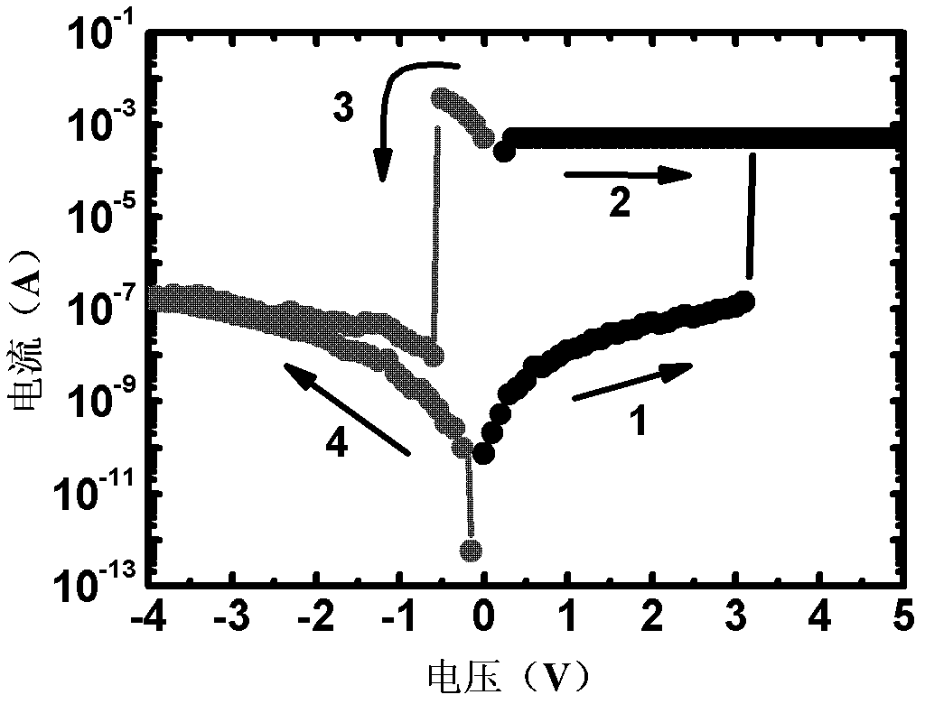
[0028] figure 1 It is the I-V characteristic diagram of the MIM structure device with Parylene-C as the middle functional layer, Al as the top electrode, and W as the bottom electrode. The mark 1 in the figure is that the device is excited by the forward voltage The transition process from high resistance state to low resistance state; 2 is the low resistance state maintenance process; 3 is the transition process of the device from low resistance state to high resistance state under the excitation of negative voltage; 4 is the high resistance state maintenance process . If the bottom electrode of the device is grounded, the voltage of the top electrode can control the resistance value of the memory, making it switch between high resistance and low resistance, that is, the transition between the two states of memory "0" and "1". The resistance ratio between the high resistance state and the low...

Embodiment 2

[0029] Example 2 Preparation of Transparent Flexible Resistive Memory

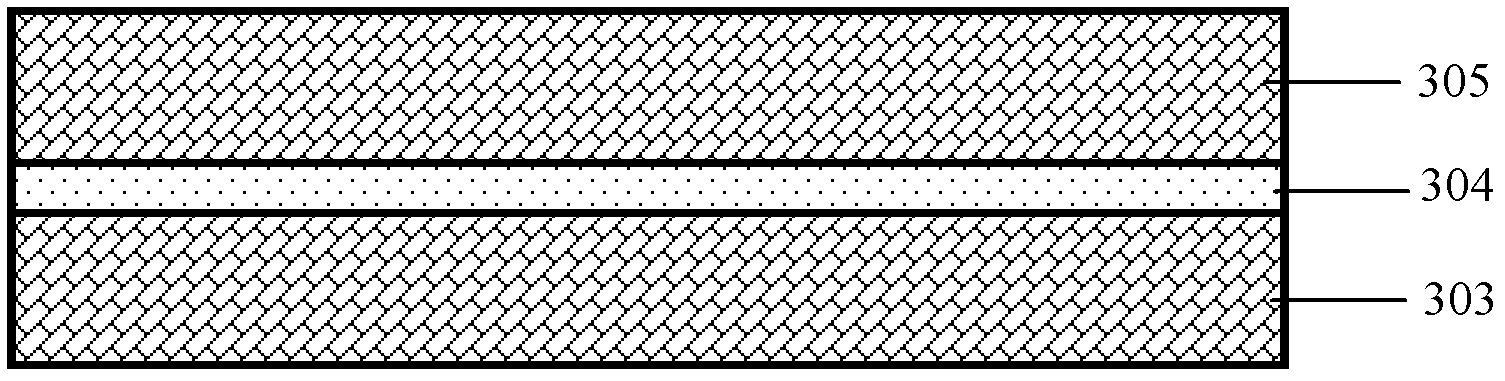
[0030] figure 2 Shown is a typical MIM capacitor structure of the transparent flexible resistive variable memory of the present invention, including a bottom electrode 303 , a middle functional layer 304 and a top electrode 305 . The preparation process of the resistive variable memory is as follows:

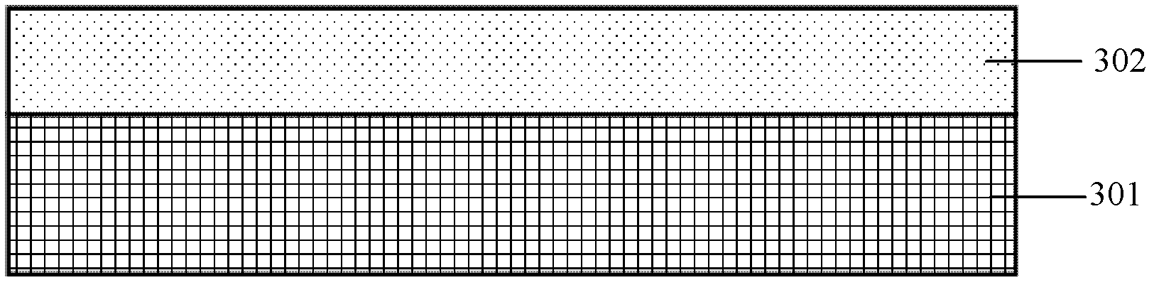
[0031] 1) Using Polymer CVD technology to grow a thick parylene-C (Parylene-C) film 302 on a silicon or glass substrate 301, with a thickness between 2 μm and 500 μm, as shown in FIG. 3(a);

[0032] 2) ITO is used as the bottom electrode 303, the bottom electrode is formed by physical vapor deposition (PVD) method or other film forming methods in IC technology, the thickness is between 200nm and 500nm, and the bottom electrode is patterned by photolithography technology , as shown in Figure 3(b) (as shown in the figure, two identical device units are fabricated on the same substrate);

[0033] 4) Utilize...


PUM


Abstract

The invention discloses a transparent flexible resistance random access memory and a manufacturing method for the transparent flexible resistance random access memory. The transparent flexible resistance random access memory comprises a transparent flexible substrate and a device unit with an MIM (metal injection molding) capacitor structure; a bottom layer and a top layer of the device unit are transparent flexible electrodes; and a middle functional layer is a poly-p-xylylene transparent film. The poly-p-xylylene material has good resistance characteristic; and the substrate, the electrodes and the middle functional layer of the device are all manufactured by a transparent flexible material so as to obtain the full-transparent flexible resistance random access memory. The transparent flexible resistance random access memory can be applied to a transparent flexible electronic system.

Description

technical field [0001] The invention belongs to flexible electronics, relates to the technical field of electronic display, polymer and CMOS hybrid integrated circuit, in particular to a transparent and flexible organic resistive random access memory (transparent and flexible organic resistive random access memory) and a manufacturing method thereof. Background technique [0002] In recent years, the development of integrated circuits has become faster and faster, and their applications have become more and more extensive. Electronic systems are being combined with more and more other types of systems to exert more powerful functions. Under this development trend, a special circuit system——flexible electronic system also came into being. Flexible electronic systems can be rolled or stretched, so they can cover any curved surface or movable parts, which greatly expands the application range of electronic systems. Among them, transparent electronic devices are widely used in f...

Claims


Application Information

Patent Timeline
Patent Type & Authority Applications(China)
IPC IPC(8): H01L45/00H01L51/00
CPCH01L51/0591H10K10/50H10N70/8845H10N70/063
Inventor 黄如唐昱蔡一茂张丽杰杨庚雨谭胜虎潘越唐粕人
Owner PEKING UNIV
Why Eureka
Try Eureka