

A kind of zno/nio heterostructure ordered porous film and preparation method thereof
A porous film and heterostructure technology, applied in the semiconductor field, can solve the problems of semiconductor devices that have not been reported, and achieve the effect of improving the overall performance, obvious rectification characteristics, and good resistance switching characteristics
- Summary
- Abstract
- Description
- Claims
- Application Information
AI Technical Summary
Problems solved by technology
Method used
Image

Examples
Embodiment 1
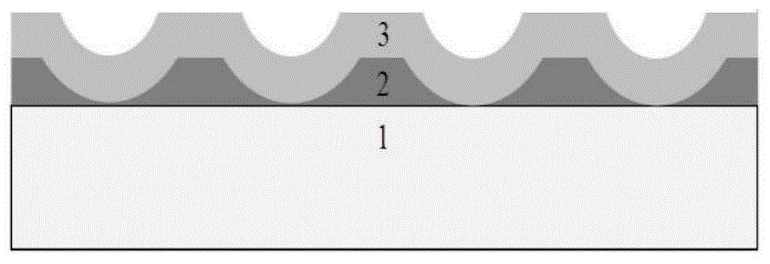
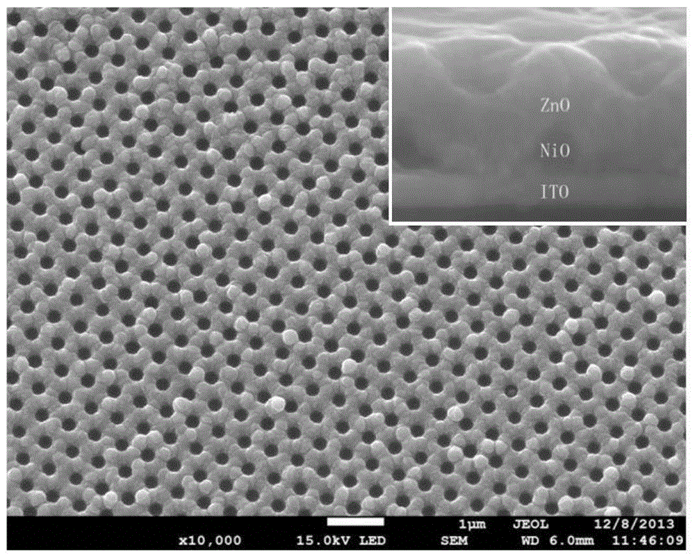
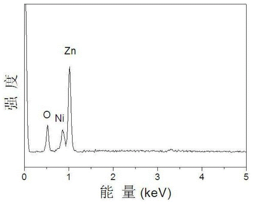
[0027] Example 1 Preparation of ZnO / NiO Heterostructure Ordered Porous Film
[0028] Step 1, first place the single-layer colloidal crystal template composed of polystyrene colloidal spheres with a diameter of 500nm on the conductive glass, and then place the conductive substrate with the single-layer colloidal crystal template on it in the nickel electrolyte to It is the working electrode, graphite is the counter electrode, and the current density is 1.0mA / cm 2 Electrodeposition by the two-electrode method was carried out for 5 minutes to obtain an ordered porous film of metallic nickel;
[0029] Step 2, place the conductive substrate grown on the ordered porous film of metallic nickel in a high-temperature tube furnace for thermal oxidation treatment, during which the high-purity O 2 The flow rate is 30sccm, the heating rate is 2°C / min, and the temperature is raised to 500°C. After maintaining the temperature for 3 hours, it is naturally cooled to room temperature. The coll...
Embodiment 2
[0034] Example 2 Preparation of ZnO / NiO Heterostructure Ordered Porous Film
[0035] Step 1, first place a single-layer colloidal crystal template composed of polystyrene colloidal spheres with a diameter of 500nm on a conductive glass substrate, and then place the conductive substrate with a single-layer colloidal crystal template on it in a nickel electrolyte , using it as the working electrode and graphite as the counter electrode, at a current density of 1.5mA / cm 2 The ordered porous film of metallic nickel was obtained by electrodepositing for 4 minutes by the two-electrode method;
[0036] Step 2, place the conductive substrate grown on the ordered porous film of metallic nickel in a high-temperature tube furnace for thermal oxidation treatment, during which the high-purity O 2 The flow rate is 40sccm, the heating rate is 4°C / min, and the temperature is raised to 500°C. After maintaining the temperature for 4 hours, it is naturally cooled to room temperature. The colloi...
Embodiment 3
[0039] Example 3 Preparation of ZnO / NiO Heterostructure Ordered Porous Film
[0040] Step 1, first place a single-layer colloidal crystal template composed of polystyrene colloidal spheres with a diameter of 500nm on a silicon wafer coated with an ITO conductive layer, and then place a conductive substrate with a single-layer colloidal crystal template on it. In the nickel electrolyte, use it as the working electrode and graphite as the counter electrode, at a current density of 2.0mA / cm 2 The ordered porous film of metallic nickel was obtained by electrodepositing for 4 minutes by the two-electrode method;
[0041] Step 2, place the conductive substrate grown on the ordered porous film of metallic nickel in a high-temperature tube furnace for thermal oxidation treatment, during which the high-purity O 2 The flow rate is 40sccm, the heating rate is 3°C / min, and the temperature is raised to 400°C. After maintaining the temperature for 3 hours, it is naturally cooled to room te...
PUM
| Property | Measurement | Unit |
|---|---|---|
| thickness | aaaaa | aaaaa |
| diameter | aaaaa | aaaaa |
| diameter | aaaaa | aaaaa |
Abstract
Description
Claims
Application Information