Printed circuit board having single reflective structure and led packaging manufacturing method utilizing the same

A technology for printed circuit boards and light-emitting diodes, applied in printed circuit manufacturing, printed circuit secondary processing, printed circuits, etc., to achieve the effects of preventing reabsorption, increasing optical power, and improving efficiency

Inactive Publication Date: 2013-01-30
斗星A-TECH +1
View PDF3 Cites 1 Cited by
  • Summary
  • Abstract
  • Description
  • Claims
  • Application Information

AI Technical Summary

Problems solved by technology

[0024] The present invention is used to solve the problems of the prior art LED packaging as described above, and its purpose is to provide a printed circuit board with a single reflective structure and a method for manufacturing a LED packaging using the same, in which the When more than one chip is used to form a light-emitting diode package, a single reflective structure is formed between the chips to prevent reabsorption of light between the chips

Method used


Image

  • Printed circuit board having single reflective structure and led packaging manufacturing method utilizing the same
  • Printed circuit board having single reflective structure and led packaging manufacturing method utilizing the same
  • Printed circuit board having single reflective structure and led packaging manufacturing method utilizing the same

Examples


Embodiment Construction

[0052] Hereinafter, preferred embodiments of the printed circuit board with a single reflective structure and the method for manufacturing an LED package using the printed circuit board according to the present invention will be described in detail.

[0053] The characteristics and advantages of the printed circuit board with a single reflective structure and the method for manufacturing a light emitting diode using the printed circuit board according to the present invention will be more clearly understood through the detailed description of the following embodiments.

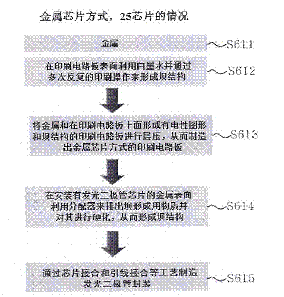
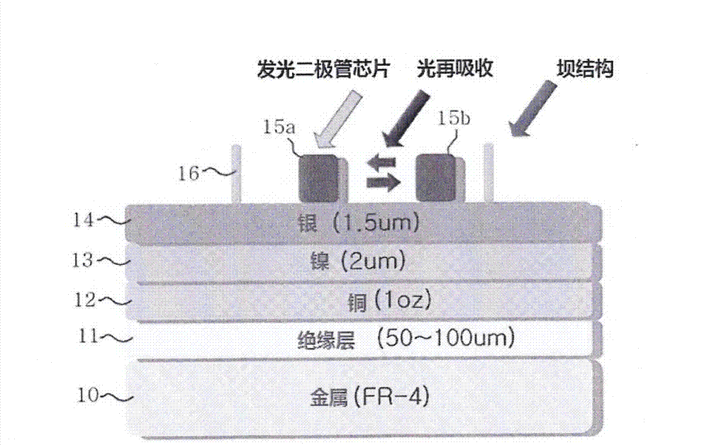
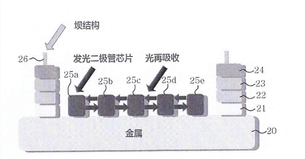
[0054] image 3 It is a composition diagram of a chip on board (Chip On Board) and a heat sink chip (Chip On Heat-sink) light emitting diode package according to an embodiment of the present invention, Figure 4 It is a configuration diagram of a chip-on-metal (Chip On Metal) light emitting diode package according to another embodiment of the present invention.

[0055] In the case of using more than one chip...


PUM


Abstract

The invention relates to a printed circuit board having a single reflective structure and an LED packaging manufacturing method utilizing the same. Under a condition that more than one chips are utilized to form LED packaging in one package, a single reflective conformation material is arranged between the chips, thereby preventing light resorption between the chips. The printed circuit board comprises the printed circuit board, a material layer which is used for forming a wiring pattern and formed on the printed circuit board, an insulation layer formed between the printed circuit board and the material layer, a dam formed on the material layer for forming the wiring pattern and a light-reabsorption-preventing dam formed on the material layer for forming the wiring pattern between LED chip areas.

Description

technical field [0001] The present invention relates to a light-emitting diode package, and more particularly to a printed circuit board with a single reflective structure and a method for manufacturing a light-emitting diode package using the same. A single reflective structure can prevent reabsorption of light between chips. Background technique [0002] A light emitting diode utilizes a p-n junction structure of a semiconductor to create injected minority carriers (electrons or holes), and it serves as an electronic component that emits light through recombination of the minority carriers. [0003] Light emitting diodes as described above are used in various fields. Recently, light emitting diodes are attracting attention as components that will replace fluorescent lamps because they have a semi-permanent lifespan and do not contain hazardous substance environmental regulations (RoHS, ELV, PFOS, etc.). [0004] Generally, a single light emitting diode unit is packaged by...

Claims


Application Information

Patent Timeline
Patent Type & Authority Applications(China)
IPC IPC(8): H05K1/18H05K1/02H05K3/30H01L25/075H01L33/48H01L33/60
CPCH01L25/075H01L24/83H01L2224/83439H05K2203/072H01L33/58H01L2924/00014H01L2924/12041H01L25/0753H01L2224/49113H05K2201/09909H01L2224/48108H05K3/30H01L2224/4805H01L2224/4909H01L2224/48091H05K3/325H01L2224/85439H01L33/48H01L24/49H01L2224/32225H01L2224/92247H05K2201/2054H01L24/48H01L24/85H01L21/58H05K1/0274H05K1/18H05K2201/10106H05K2201/0338H01L24/32H01L2224/48227H01L2224/4912H01L33/60H05K1/02H01L24/92H05K1/021H01L2224/73265H05K3/28H05K1/181H01L2224/48137H01L2224/45099H01L2224/29099H01L2924/00
Inventor 张种镇
Owner 斗星A-TECH
Why Eureka
Try Eureka