Manufacturing method for nanowire single-photon detector based on specially doped superconducting niobium film material

A single-photon detector and thin-film material technology, which is applied in semiconductor devices, metal material coating technology, ion implantation plating, etc., can solve the problems of low superconducting transition temperature, small critical current density, and short photoresponse wavelength. The effect of achieving a high critical current density

Active Publication Date: 2013-02-06
NANJING UNIV
View PDF4 Cites 26 Cited by
  • Summary
  • Abstract
  • Description
  • Claims
  • Application Information

AI Technical Summary

Problems solved by technology

The pure Nb material currently studied, because of its low superconducting transition temperature, low critical current density,

Method used


Image

  • Manufacturing method for nanowire single-photon detector based on specially doped superconducting niobium film material
  • Manufacturing method for nanowire single-photon detector based on specially doped superconducting niobium film material
  • Manufacturing method for nanowire single-photon detector based on specially doped superconducting niobium film material

Examples


Embodiment Construction

[0029] Below in conjunction with accompanying drawing and specific embodiment, further illustrate the present invention, should be understood that these embodiments are only for illustrating the present invention and are not intended to limit the scope of the present invention, after having read the present invention, those skilled in the art will understand various aspects of the present invention Modifications in equivalent forms all fall within the scope defined by the appended claims of this application.

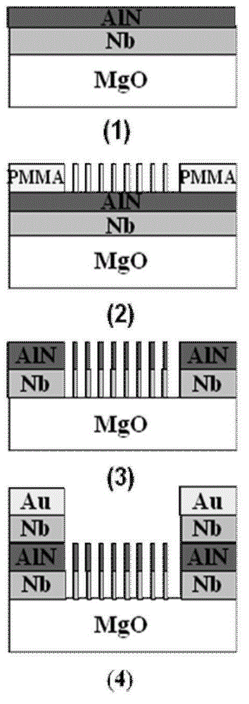
[0030] Concrete micromachining manufacturing steps of the present invention are:

[0031] 1. First put the double-sided polished MgO substrate (referred to as "substrate") into the acetone solution for ultrasonic cleaning for 3 to 5 minutes, then put the substrate into the alcohol solution for ultrasonic cleaning for 3 to 5 minutes, and finally use deionized Ultrasonic cleaning with water for 3 to 5 minutes, drying the substrate with nitrogen gas, checking the cleanlines...


PUM


Abstract

The invention discloses a manufacturing method for a nanowire single-photon detector based on a specially doped superconducting niobium film material. The manufacturing method comprises the following steps: carrying out ultrasonic cleaning and blow-drying on a substrate; carrying out Ar ion cleaning; growing a specially doped superconducting Nb film in a direct current magnetron sputtering way; carrying out spin-coating on an electron beam resist, carrying out electron beam lithography on the electron beam resist, and drawing a wire pattern with the width not more than 100nm on the electron beam resist; etching in a reaction ion etching way, and transferring the line pattern onto the Nb film to form a Nb nanowire; cleaning the residual electron beam resist, carrying out spin-coating on a photoresist on the surface of a sample, and forming an electrode pattern on the photoresist in a deep ultraviolet exposure way; and growing an electrode. According to the manufacturing method, the difficult problems of low superconducting transition temperature, low critical current density and short photoresponse wavelength of an SNSPD (Superconducting Nanowire Single Photon Detector) manufactured by the conventional Nb material are solved.

Description

technical field [0001] The invention relates to a preparation method of a highly sensitive single photon or extremely weak light signal detector, in particular to a preparation method of a nanowire single photon detector based on a specially doped superconducting niobium thin film material, which can be applied to infrared And the detection of single photon or extremely weak light signal in the far infrared band. Background technique [0002] At present, NbN-based superconducting nanowire single photon detector (Superconducting Nanowire Single Photon Detector, referred to as SNSPD) has been relatively mature, its high superconducting transition temperature (~12K), low dark count rate (10c / s), Small time jitter (60ps), wide response spectrum (404nm~1550nm), fast repetition rate (>100MHz) and other characteristics make it widely used in quantum key distribution, integrated circuit detection and other fields. Recently, in addition to NbN materials, many other superconductin...

Claims


Application Information

Patent Timeline
IPC IPC(8): H01L31/18C23C14/35C23C14/18C23C14/06C23C14/54
CPCC23C14/021C23C14/185
Inventor 康琳郏涛贾小氢张蜡宝吴培亨
Owner NANJING UNIV
Why Eureka
Try Eureka